Datasheet 搜索 > 稳压芯片 > TI(德州仪器) > TPS7A8101QDRBRQ1 数据手册 > TPS7A8101QDRBRQ1 产品设计参考手册 4/9 页
 器件3D模型
¥ 5.767
TPS7A8101QDRBRQ1 产品设计参考手册 - TI(德州仪器)
制造商:
TI(德州仪器)
分类:
稳压芯片
封装:
VDFN-8
描述:
TPS7A8101QDRBRQ1 编带
Pictures:
3D模型
符号图
焊盘图
引脚图
产品图
页面导航:
原理图在P7
焊盘布局在P4
应用领域在P9
型号编号列表在P5

导航目录
TPS7A8101QDRBRQ1数据手册
Page:
of 9 Go
若手册格式错乱,请下载阅览PDF原文件
Iout
Vout
Iout
Vout
PG
EN
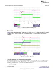
Thermal Guidelines and Layout Recommendations
www.ti.com
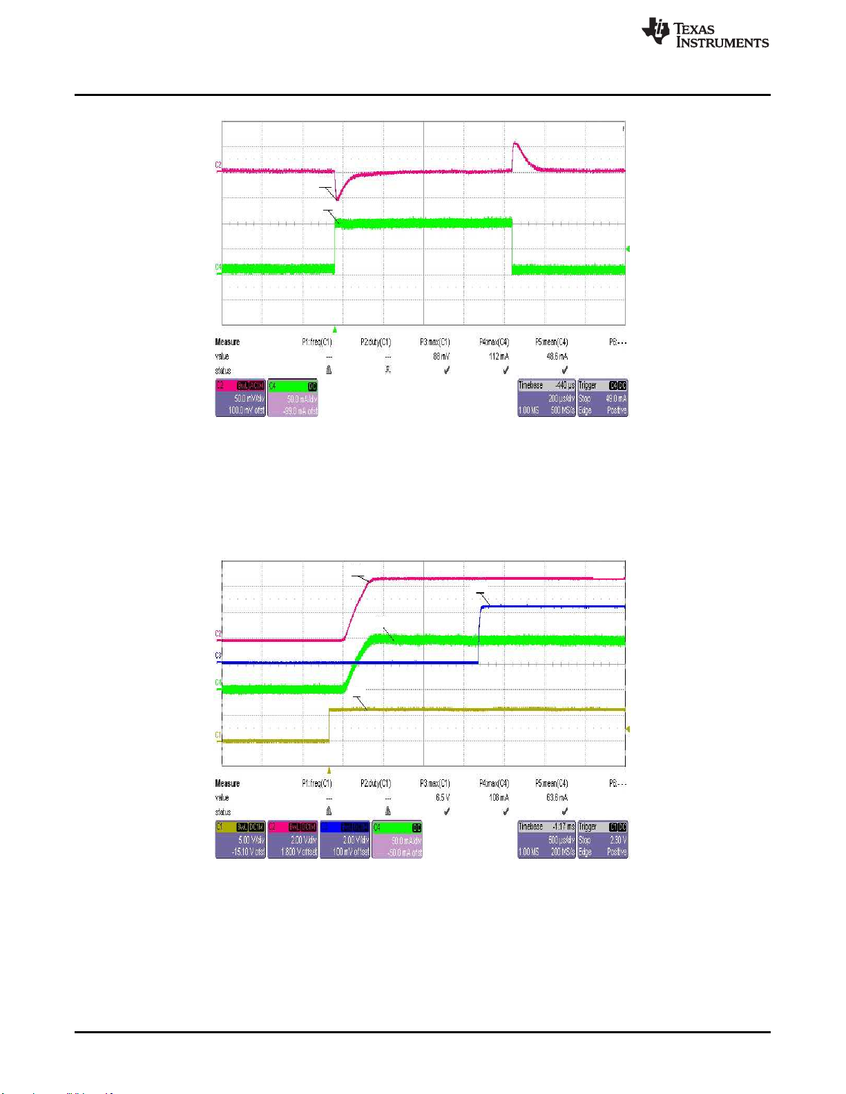
Figure 2. Load Step and Transient Response
4.3 Power Good
Figure 3 shows the operation of the Power Good (PG) output. Vin (6 V) is present and the chip is enabled
(c1, gold) The PG output (C3, blue) goes HIGH approximately 1.5 ms after Vout (C2, red) goes into
regulation.
Figure 3. Power Good Operation
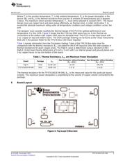
5 Thermal Guidelines and Layout Recommendations
Thermal management is a key component of design for any power converter and is especially important
when the power dissipation in the LDO regulator is high. Use the following formula to approximate the
maximum power dissipation for the particular ambient temperature:
T
J
= T
A
+ P
D
× θ
JA
4
TPS7A1601EVM-046 SLVU549– December 2011
Submit Documentation Feedback
Copyright © 2011, Texas Instruments Incorporated
器件 Datasheet 文档搜索
AiEMA 数据库涵盖高达 72,405,303 个元件的数据手册,每天更新 5,000 多个 PDF 文件
