Datasheet 搜索 > 开发套件 > TI(德州仪器) > CDCEL949PERF-EVM 数据手册 > CDCEL949PERF-EVM 用户编程技术手册 1/41 页

¥ 1289.202
CDCEL949PERF-EVM 用户编程技术手册 - TI(德州仪器)
制造商:
TI(德州仪器)
分类:
开发套件
描述:
TEXAS INSTRUMENTS CDCEL949PERF-EVM 评估模块, 时钟发生器, CDCEL949
Pictures:
3D模型
符号图
焊盘图
引脚图
产品图
页面导航:
引脚图在P4P5Hot
典型应用电路图在P1P27P28P29P30P31
原理图在P1P13
封装尺寸在P35P37P38
标记信息在P35P36
封装信息在P34P35P36P37P38
技术参数、封装参数在P5
应用领域在P1P41
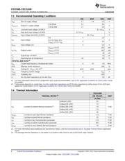
电气规格在P7P8
导航目录
CDCEL949PERF-EVM数据手册
Page:
of 41 Go
若手册格式错乱,请下载阅览PDF原文件
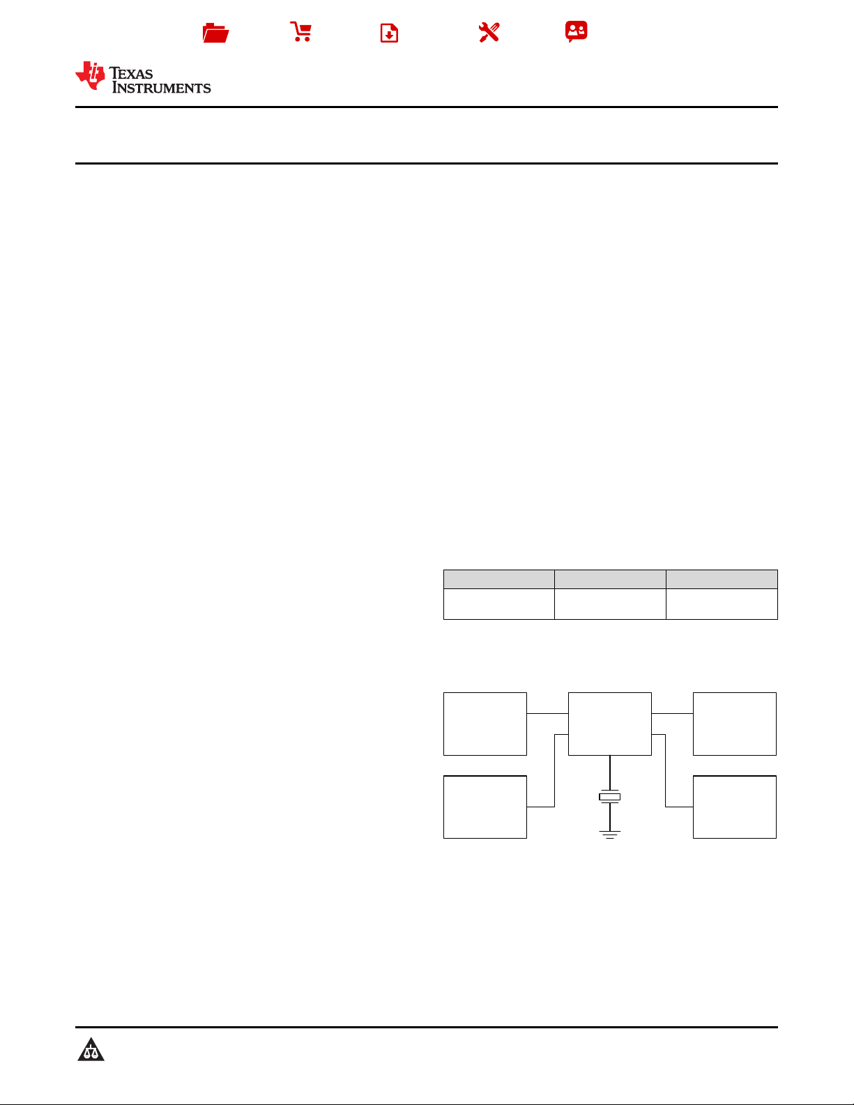
CDCE(L)9xx
Clock
Ethernet
PHY
USB
Controller
WiFi
FPGA
25
MHz
Copyright © 2016, Texas Instruments Incorporated
Product
Folder
Sample &
Buy
Technical
Documents
Tools &
Software
Support &
Community
An IMPORTANT NOTICE at the end of this data sheet addresses availability, warranty, changes, use in safety-critical applications,
intellectual property matters and other important disclaimers. PRODUCTION DATA.
CDCE949
,
CDCEL949
SCAS844F –AUGUST 2007–REVISED OCTOBER 2016
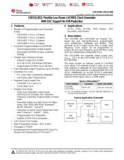
CDCE(L)913: Flexible Low Power LVCMOS Clock Generator
With SSC Support for EMI Reduction
1
1 Features
1
• Member of Programmable Clock Generator
Family
– CDCEx913: 1 PLLs, 3 Outputs
– CDCEx925: 2 PLLs, 5 Outputs
– CDCEx937: 3 PLLs, 7 Outputs
– CDCEx949: 4 PLLs, 9 Outputs
• In-System Programmability and EEPROM
– Serial Programmable Volatile Register
– Nonvolatile EEPROM to Store Customer
Settings
• Flexible Input Clocking Concept
– External Crystal: 8 to 32 MHz
– On-Chip VCXO: Pull-Range ±150 ppm
– Single-Ended LVCMOS Up to 160 MHz
• Free Selectable Output Frequency Up to 230 MHz
• Low-Noise PLL Core
– PLL Loop Filter Components Integrated
– Low Period Jitter (Typical 60 ps)
• Separate Output Supply Pins
– CDCE949: 3.3 V and 2.5 V
– CDCEL949: 1.8 V
• Flexible Clock Driver
– Three User-Definable Control Inputs
[S0/S1/S2], for Example, SSC Selection,
Frequency Switching, Output Enable or Power
Down
– Generates Highly Accurate Clocks for Video,
Audio, USB, IEEE1394, RFID, Bluetooth
®
,
WLAN, Ethernet™, and GPS
– Generates Common Clock Frequencies Used
With TI-DaVinci™, OMAP™, DSPs
– Programmable SSC Modulation
– Enables 0-PPM Clock Generation
• 1.8-V Device Core Supply
• Wide Temperature Range: –40°C to 85° C
• Packaged in TSSOP
• Development and Programming Kit for Easy PLL
Design and Programming (TI Pro-Clock™)
2 Applications
D-TVs, STBs, IP-STBs, DVD Players, DVD
Recorders, and Printers
3 Description
The CDCE949 and CDCEL949 are modular PLL-
based low cost, high-performance, programmable
clock synthesizers, multipliers and dividers. They
generate up to 9 output clocks from a single input
frequency. Each output can be programmed in-
system for any clock frequency up to 230 MHz, using
up to four independent configurable PLLs.
The CDCEx949 has separate output supply pins,
V
DDOUT
, 1.8 V for the CDCEL949, and 2.5 V to 3.3 V
for CDCE949.
The input accepts an external crystal or LVCMOS
clock signal. If an external crystal is used, an on-chip
load capacitor is adequate for most applications. The
value of the load capacitor is programmable from 0 to
20 pF. Additionally, an on-chip VCXO is selectable,
allowing synchronization of the output frequency to an
external control signal, that is, a PWM signal.
Device Information
(1)
PART NUMBER PACKAGE BODY SIZE (NOM)
CDCE949
CDCEL949
TSSOP (24) 7.80 mm × 4.40 mm
(1) For all available packages, see the orderable addendum at
the end of the data sheet.
Typical Application Schematic
器件 Datasheet 文档搜索
AiEMA 数据库涵盖高达 72,405,303 个元件的数据手册,每天更新 5,000 多个 PDF 文件
