Datasheet 搜索 > 运算放大器 > Burr Brown > INA145UA/2K5 数据手册 > INA145UA/2K5 用户编程技术手册 2/15 页

 器件3D模型
¥ 0
INA145UA/2K5 用户编程技术手册 - Burr Brown
制造商:
Burr Brown
分类:
运算放大器
封装:
SOIC
Pictures:
3D模型
符号图
焊盘图
引脚图
产品图
页面导航:
封装尺寸在P12P13P14
封装信息在P12P13P14
技术参数、封装参数在P2P3
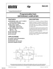
应用领域在P1P15
导航目录
INA145UA/2K5数据手册
Page:
of 15 Go
若手册格式错乱,请下载阅览PDF原文件

2
®
INA145
The information provided herein is believed to be reliable; however, BURR-BROWN assumes no responsibility for inaccuracies or omissions. BURR-BROWN assumes
no responsibility for the use of this information, and all use of such information shall be entirely at the user’s own risk. Prices and specifications are subject to change
without notice. No patent rights or licenses to any of the circuits described herein are implied or granted to any third party. BURR-BROWN does not authorize or warrant
any BURR-BROWN product for use in life support devices and/or systems.
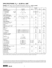
INA145UA
PARAMETER CONDITION MIN TYP MAX UNITS
OFFSET VOLTAGE, V
O
RTI
(1, 2)
Input Offset Voltage V
OS
V
CM
= V
O
= 0V ±0.2 ±1mV
vs Temperature ∆V
OS
/∆T See Typical Curve
vs Power Supply PSRR V
S
= ±1.35V to ±18V ±20 ±60 µV/V
vs Time ±0.3 µV/mo
Offset Voltage, V
01
RTI
(1, 2)
±0.4 mV
INPUT VOLTAGE RANGE
Common-Mode Voltage Range V
CM
(V
IN
+) – (V
IN
–) = 0V, V
O
= 0V 2(V–) 2(V+) –2 V
Common-Mode Rejection CMRR V
CM
= 2(V–) to 2(V+) – 2V, R
S
= 0Ω 76 86 dB
Over Temperature V
S
= ±15V 70 80 dB
INPUT BIAS CURRENT
(2)
V
CM
= V
S
/2
Bias Current I
B
±50 nA
Offset Current I
OS
±5nA
INPUT IMPEDANCE
Differential (non-inverting input) 80 kΩ
Differential (inverting input) 27 kΩ
Common-Mode 40 kΩ
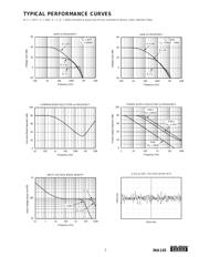
NOISE RTI
(1, 3)
Voltage Noise, f = 0.1Hz to 10Hz 2 µVp-p
Voltage Noise Density, f = 1kHz e
n
90 nV/√Hz
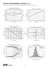
GAIN
G = 1 to 1000
Gain Equation G = 1 + R
G2
/R
G1
V/V
Initial
(1)
1V/V
Gain Error R
L
= 100kΩ, V
O
= (V–)+0.15 to (V+)–1, G = 1 ±0.01 ±0.1 %
vs Temperature R
L
= 100kΩ, V
O
= (V–)+0.25 to (V+)–1, G = 1 ±2 ±10 ppm/°C
R
L
= 10kΩ, V
O
= (V–)+0.3 to (V+)–1.25, G = 1 ±0.01 ±0.1 %
vs Temperature R
L
= 10kΩ, V
O
= (V–)+0.5 to (V+)–1.25, G = 1 ±2 ±10 ppm/°C
Nonlinearity R
L
= 10kΩ, V
O
= (V–)+0.3 to (V+)–1.25, G = 1 ±0.0002 ±0.005 % of FS
FREQUENCY RESPONSE
Small Signal Bandwidth G = 1 500 kHz
G = 10 50 kHz
Slew Rate 0.45 V/µs
Settling Time, 0.1% G = 1, 10V Step 40 µs
0.01% G = 1, 10V Step 90 µs
Overload Recovery 50% Input Overload 40 µs
OUTPUT, V
O
Voltage Output R
L
= 100kΩ, G = 1 (V–) + 0.15 (V+) – 1 V
Over Temperature R
L
= 100kΩ, G = 1 (V–) + 0.25 (V+) – 1 V
R
L
= 10kΩ, G = 1 (V–) + 0.3 (V+) – 1.25 V
Over Temperature R
L
= 10kΩ, G = 1 (V–) + 0.5 (V+) – 1.25 V
Short-Circuit Current Continuous to Common ±15 mA
Capacitive Load Stable Operation 1000 pF
POWER SUPPLY
Specified Voltage Range, Dual Supplies ±2.25 ±18 V
Operating Voltage Range ±1.35 ±18 V
Quiescent Current V
IN
= 0, I
O
= 0 ±570 ±700 µA
Over Temperature
±800 µA
TEMPERATURE RANGE
Specified Range –40 +85 °C
Operating Range –55 +125 °C
Storage Range –55 +125 °C
Thermal Resistance
θ
JA
150 °C/W
NOTES: (1) Referred to input pins (V
IN
+ and V
IN
–), Gain = 1V/V. Specified with 10kΩ in feedback of A2. (2) Input offset voltage specification includes effects of amplifier’s
input bias and offset currents. (3) Includes effects of input bias current noise and thermal noise contribution of resistor network.
SPECIFICATIONS: V
S
= ±2.25V to ±18V
Boldface limits apply over the specified temperature range, T
A
= –40°C to +85°C
At T
A
= +25°C, G = 1, R
L
= 10kΩ connected to ground and ref pin connected to ground unless otherwise noted.
器件 Datasheet 文档搜索
AiEMA 数据库涵盖高达 72,405,303 个元件的数据手册,每天更新 5,000 多个 PDF 文件
