Datasheet 搜索 > 运算放大器 > Burr Brown > INA145UA/2K5 数据手册 > INA145UA/2K5 用户编程技术手册 4/15 页

 器件3D模型
¥ 0
INA145UA/2K5 用户编程技术手册 - Burr Brown
制造商:
Burr Brown
分类:
运算放大器
封装:
SOIC
Pictures:
3D模型
符号图
焊盘图
引脚图
产品图
页面导航:
封装尺寸在P12P13P14
封装信息在P12P13P14
技术参数、封装参数在P2P3
应用领域在P1P15
导航目录
INA145UA/2K5数据手册
Page:
of 15 Go
若手册格式错乱,请下载阅览PDF原文件
4
®
INA145
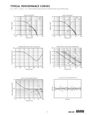
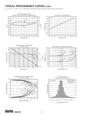
AMPLIFIER A1, A2 PERFORMANCE
Boldface limits apply over the specified temperature range, T
A
= –40°C to +85°C
At T
A
= +25°C, G = 1, R
L
= 10kΩ connected to ground and ref pin connected to ground unless otherwise noted.
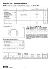
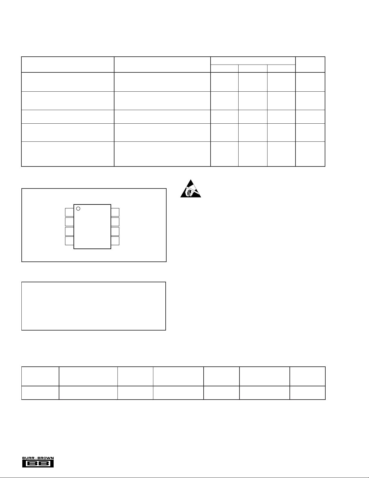
PIN CONFIGURATION
ELECTROSTATIC
DISCHARGE SENSITIVITY
This integrated circuit can be damaged by ESD. Burr-Brown
recommends that all integrated circuits be handled with
appropriate precautions. Failure to observe proper handling
and installation procedures can cause damage.
ESD damage can range from subtle performance degradation
to complete device failure. Precision integrated circuits may
be more susceptible to damage because very small parametric
changes could cause the device not to meet its published
specifications.
Supply Voltage, V+ to V–.................................................................... 36V
Signal Input Terminals, Voltage ........................................................ ±80V
Current ....................................................... ±1mA
Output Short Circuit (to ground).............................................. Continuous
Operating Temperature ..................................................–55°C to +125°C
Storage Temperature .....................................................–55°C to +150°C
Junction Temperature.................................................................... +150°C
Lead Temperature (soldering, 10s)............................................... +240°C
NOTE: (1) Stresses above these ratings may cause permanent damage.
Exposure to absolute maximum conditions for extended periods may degrade
device reliability.
ABSOLUTE MAXIMUM RATINGS
(1)
Top View SO-8
PACKAGE SPECIFIED
DRAWING TEMPERATURE PACKAGE ORDERING TRANSPORT
PRODUCT PACKAGE NUMBER RANGE MARKING NUMBER
(1)
MEDIA
INA145UA SO-8 182 –40°C to +85°C INA145UA INA145UA Rails
"""""INA145UA/2K5 Tape and Reel
NOTE: (1) Models with a slash (/) are available only in Tape and Reel in the quantities indicated (e.g., /2K5 indicates 2500 devices per reel). Ordering 2500 pieces
of “INA145UA/2K5” will get a single 2500-piece Tape and Reel.
PACKAGE/ORDERING INFORMATION
INA145UA
PARAMETER CONDITION MIN TYP MAX UNITS
OFFSET VOLTAGE, V
O
RTI
(1, 2)
Input Offset Voltage V
OS
V
S
= ±15V, V
CM
= V
O
= 0V ±0.5 mV
vs Temperature ∆V
OS
/∆T ±1 µV/°C
INPUT VOLTAGE RANGE
Common-Mode Voltage Range V
CM
V
IN
+ – V
IN
– = 0V, V
O
= 0V (V–) to (V+) –1 V
Common-Mode Rejection Ratio CMRR V
CM
= (V–) to (V+) –1 90 dB
OPEN-LOOP GAIN
Open Loop Gain A
OL
110 dB
INPUT BIAS CURRENT
(2)
Bias Current I
B
±50 nA
Offset Current I
OS
±5nA
RESISTOR AT A1 OUTPUT, V
O1
Initial 10 kΩ
Error ±0.2 %
Temperature Drift Coefficient ±50 ppm/°C
Ref
V
IN
V
IN
V–
–
+
V
O1
V+
V
O
R
G
1
2
3
4
8
7
6
5
器件 Datasheet 文档搜索
AiEMA 数据库涵盖高达 72,405,303 个元件的数据手册,每天更新 5,000 多个 PDF 文件
