Datasheet 搜索 > 微处理器 > NXP(恩智浦) > P1013NXN2HFB 数据手册 > P1013NXN2HFB 用户编程技术手册 6/35 页

¥ 1204.098
P1013NXN2HFB 用户编程技术手册 - NXP(恩智浦)
制造商:
NXP(恩智浦)
分类:
微处理器
封装:
BGA-689
描述:
PowerPC系列 1.055GHz
Pictures:
3D模型
符号图
焊盘图
引脚图
产品图


P1013NXN2HFB数据手册
Page:
of 35 Go
若手册格式错乱,请下载阅览PDF原文件
PowerQUICC and QorIQ DDR3 SDRAM Controller Register Setting Considerations, Rev. 4
6 Freescale Semiconductor
Register definitions
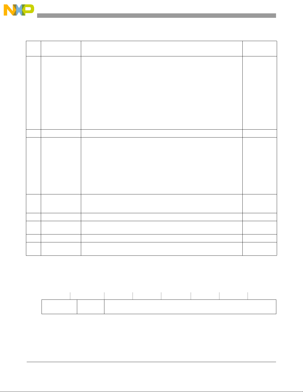
2.3 Chip-Select n Configuration 2 Register (CSn_CONFG_2)
The chip-select n configuration 2 register (CSn_CONFG_2) is shown in Figure 3.
9–11 ODT_RD_CFG ODT for reads configuration
This setting is topology-dependent. During the read cycle, the memory controller
is the target and DDR3 memory is the source. Typically, for one DIMM module,
ODT is disabled for reads. For two modules, ODT is asserted to the standby
module (the DIMM that is not active) during reads. In addition, regardless of
whether one or two modules are used only during reads, the on-chip ODT is
asserted to memory controller (enabled through
DDR_SDRAM_CFG2[ODT_CFG]). Therefore, this field, which controls assertion
of the ODT signal to DDR3 memory during the read, is typically disabled for one
module and enabled for two modules for the inactive module. This is not a
requirement, and DRAM vendor documents need to be consulted for
vendor-specific recommendation. For further information on DRAM ODT settings,
see the Micron technical note “tn_41_08” available on their website.
Application
dependent
12 — Reserved —
13–15 ODT_WR_CFG ODT for writes configuration
During the write cycle, the memory controller is the source and DDR3 memory is
the target. For one DIMM module with one rank, assert the ODT to the active
module. For one DIMM module with two rank, assert the ODT only to rank1 to the
active module. For two DIMM modules, assert the ODT to the standby module. The
reason for asserting or not asserting ODT is to balance the line impedance
between the source and the target to avoid unwanted reflections of signals. This is
not a requirement, and DRAM vendor documents need to be consulted for vendor
specific recommendation. For further information on DRAM ODT settings, see the
Micron technical note “tn_41_08” available on their website.
1 —> Assert
ODT only during
writes to CS0.
16–17 BA_BITS_CS_n Number of bank bits for SDRAM on chip-select n
The value of number of banks is obtained from the memory manufacturer’s data
sheet. For DDR3, eight banks are typically selected.
—
18–20 — Reserved —
21–23 ROW_BITS_CS_n Number of row bits for SDRAM on chip-select n
The number of rows is obtained from the memory manufacturer’s data sheet.
—
24–28 — Reserved —
29–31 COL_BITS_CS_n Number of column bits for SDRAM on chip-select n
The number of columns is obtained from the memory manufacturer’s data sheet.
—
Offset 0x0C0 Access: Read/Write
04578 31
R
— PARS_CFG —
W
Figure 3. Chip-Select n Configuration 2 Register (CSn_CONFG_2)
Table 3. CS_n CONFIG Register field descriptions (continued)
Bits Name Description
Recommended
settings
器件 Datasheet 文档搜索
AiEMA 数据库涵盖高达 72,405,303 个元件的数据手册,每天更新 5,000 多个 PDF 文件
