Datasheet 搜索 > 8位微控制器 > Microchip(微芯) > PIC16F526-E/P 数据手册 > PIC16F526-E/P 用户编程技术手册 2/22 页
 器件3D模型
¥ 1.265
PIC16F526-E/P 用户编程技术手册 - Microchip(微芯)
制造商:
Microchip(微芯)
分类:
8位微控制器
封装:
PDIP-14
描述:
14引脚, 8位闪存微控制器 14-Pin, 8-Bit Flash Microcontroller
Pictures:
3D模型
符号图
焊盘图
引脚图
产品图
页面导航:
引脚图在P1Hot
技术参数、封装参数在P17
电气规格在P17P19
导航目录
PIC16F526-E/P数据手册
Page:
of 22 Go
若手册格式错乱,请下载阅览PDF原文件
PIC16F526
DS41317B-page 2 © 2007 Microchip Technology Inc.
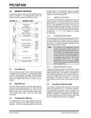
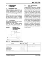
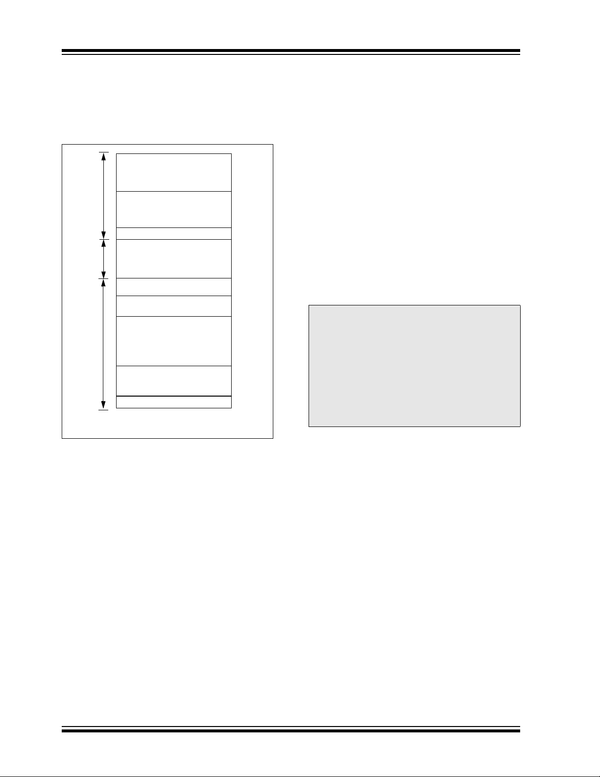
2.0 MEMORY MAPPING
The Program Memory map of the PIC16F526 device is
shown in Figure 2-1. In Program/Verify mode, the
Program Memory extends from 0x000 to 0x7FF.
FIGURE 2-1: MEMORY MAP
2.1 User Memory
The user memory space is the on-chip user program
memory. As shown in Figure 2-1, it extends from 0x000
to 0x3FF and partitions into pages, including Reset
vector at address 0x3FF. Note that the PC will incre-
ment from (0x000-0x3FF) then to 0x400, (not to
0x000).
2.2 Data Memory
The data memory space is the Flash data memory
block and is located at addresses PC = 400h-43Fh. All
program mode commands that work on the normal
Flash memory work on the Flash data memory block.
This includes Bulk Erase, Load and Read Data
commands.
2.3 Configuration Memory
The configuration memory space extends from 0x440
to 0x7FF. Locations from 0x448 through 0x49F are
reserved. The user ID locations extend from 0x440
through 0x443. The Configuration Word is physically
located at 0x7FF, and the backup OSCCAL locations
extend from 0x444 through 0x447.
2.3.1 USER ID LOCATIONS
A user may store identification information (ID) in four
user ID locations. The user ID locations are mapped in
[0x440:0x443]. It is recommended that users use only
the four Least Significant bits (LSb) of each user ID
location and program the upper 8 bits as ‘1’s. The user
ID locations read out normally, even after code protec-
tion is enabled. It is recommended that user ID location
is written as ‘1111 1111 bbbb’ where ‘bbbb’ is user
ID information.
2.3.2 CONFIGURATION WORD
The Configuration Word is physically located at 0x7FF.
It is only available upon Program mode entry. Once an
Increment Address command is issued, the Configura-
tion Word is no longer accessible, regardless of the
address of the program counter.
2.3.3 BACKUP OSCCAL VALUE
The backup OSCCAL locations, 0x444-0x447, are the
locations where the OSCCAL values are stored during
testing of the INTOSC. This location is not erased dur-
ing a standard Bulk Erase, but is erased if the PC is
moved into configuration memory prior to invoking a
Bulk Erase. If this value is erased, it is the user’s
responsibility to rewrite it back to this location for future
use.
2.4 Oscillator Calibration Bits
The oscillator Calibration bits are stored at the Reset
vector as the operand of a MOVLW instruction. Program-
ming interfaces must allow users to program the
Calibration bits themselves for custom trimming of the
INTOSC. Capability for programming the Calibration
bits when programming the entire memory array must
also be maintained for backwards compatibility.
000h
1FFh
Reset Vector
On-chip User
Program
Memory (Page 0)
200h
3FFh
3FEh
User ID Locations
Reserved
Configuration Word
400h
443h
444h
7FEh
7FFh
43Fh
440h
Unimplemented
On-chip User
Program
Memory (Page 1)
Data Memory
Flash Data Memory
448h
49Fh
Backup OSCCAL
Locations
447h
4A0h
Configuration Memory
Space
Space
User Memory
Space
Note: By convention, the Configuration Word is
stored at the logical address location of
0xFFF within the hex file generated for the
PIC16F526. This logical address location
may not reflect the actual physical address
for the part itself. It is the responsibility of
the programming software to retrieve the
Configuration Word from the logical
address within the hex file and granulate
the address to the proper physical location
when programming.
器件 Datasheet 文档搜索
AiEMA 数据库涵盖高达 72,405,303 个元件的数据手册,每天更新 5,000 多个 PDF 文件
