Datasheet 搜索 > 8位微控制器 > Microchip(微芯) > PIC16F526-E/P 数据手册 > PIC16F526-E/P 用户编程技术手册 3/22 页
 器件3D模型
¥ 9.095
PIC16F526-E/P 用户编程技术手册 - Microchip(微芯)
制造商:
Microchip(微芯)
分类:
8位微控制器
封装:
PDIP-14
描述:
14引脚, 8位闪存微控制器 14-Pin, 8-Bit Flash Microcontroller
Pictures:
3D模型
符号图
焊盘图
引脚图
产品图
页面导航:
引脚图在P1Hot
技术参数、封装参数在P17
电气规格在P17P19
导航目录
PIC16F526-E/P数据手册
Page:
of 22 Go
若手册格式错乱,请下载阅览PDF原文件
© 2007 Microchip Technology Inc. DS41317B-page 3
PIC16F526
3.0 COMMANDS AND
ALGORITHMS
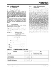
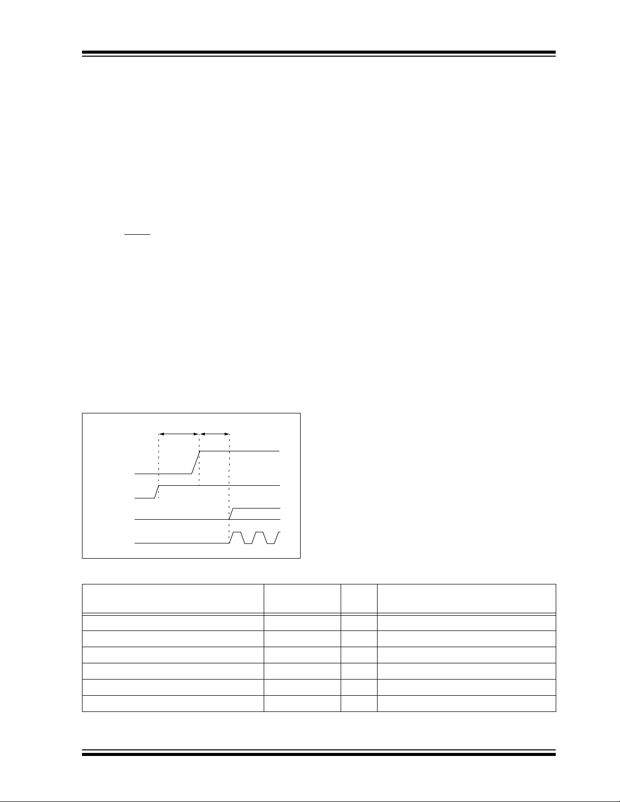
3.1 Program/Verify Mode
The Program/Verify mode is entered by holding pins
ICSPCLK and ICSPDAT low while raising V
DD pin from
V
IL to VDD. Then raise VPP from VIL to VIHH. Once in
this mode, the user program memory and configuration
memory can be accessed and programmed in serial
fashion. Clock and data are Schmitt Trigger input in this
mode.
The sequence that enters the device into the Program-
ming/Verify mode places all other logic into the Reset
state (the MCLR
pin was initially at VIL). This means
that all I/Os are in the Reset state (high-impedance
inputs).
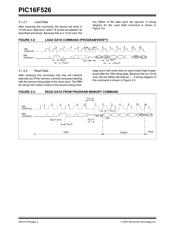
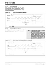
3.1.1 PROGRAMMING
The programming sequence loads a word, programs,
verifies and finally increments the PC.
Program/Verify mode entry will set the address to
0x7FF. The Increment Address command will
increment the PC. The available commands are shown
in Table 3-1.
FIGURE 3-1: ENTERING HIGH
VOLTAGE PROGRAM/
VERIFY MODE
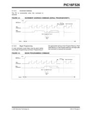
3.1.2 SERIAL PROGRAM/VERIFY
OPERATION
The RB1 pin is used as a clock input pin, and the RB0
pin is used for entering command bits and data input/
output during serial operation. To input a command, the
clock pin (RB1) is cycled 6 times. Each command bit is
latched on the falling edge of the clock with the Least
Significant bit (LSb) of the command being input first.
The data on pin RB0 is required to have a minimum
setup and hold time of 100 ns with respect to the falling
edge of the clock. Commands that have data associ-
ated with them (Read and Load) are specified to have
a minimum delay of 1 µs between the command and
the data. After this delay the clock pin is cycled 16 times
with the first cycle being a Start bit and the last cycle
being a Stop bit. Data is also input and output LSb first,
with data input being latched on the falling edge of the
clock and data output being driven on the rising edge of
the clock. Therefore, during a Read operation the LSb
will be transmitted onto pin RB0 on the rising edge of
the second cycle, and during a Load operation the LSb
will be latched on the falling edge of the second cycle.
A minimum 1 µs delay is also specified between con-
secutive commands; except the “End Programming”
command which requires a 100 µs delay. Because this
is a 12-bit core, the two MSbs of the data word are
ignored. The commands that are available are
described in Table 3-1.
TABLE 3-1: COMMAND MAPPING LOAD DATA
VPP
THLD0
VDD
TPPDP
RB1
(ICSPCLK)
(ICSPDAT)
RB0
Command
Mapping
(MSb ... LSb)
Hex
Value
Data
Load Data X X 0 0 1 0 2 start_bit, data (14), stop_bit
Read Data X X 0 1 0 0 4 start_bit, data (14), stop_bit
Increment Address X X 0 1 1 0 6
Begin Programming X X 1 0 0 0 8
End Programming X X 1 1 1 0 E
Bulk Erase Program Memory X X 1 0 0 1 9
器件 Datasheet 文档搜索
AiEMA 数据库涵盖高达 72,405,303 个元件的数据手册,每天更新 5,000 多个 PDF 文件
