Datasheet 搜索 > 微控制器 > Microchip(微芯) > PIC16F628A-I/ML 数据手册 > PIC16F628A-I/ML 用户编程技术手册 3/22 页
 器件3D模型
¥ 27.397
PIC16F628A-I/ML 用户编程技术手册 - Microchip(微芯)
制造商:
Microchip(微芯)
分类:
微控制器
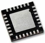
封装:
QFN-28
描述:
PIC16F627A/628A/648A 微控制器Microchip 的 PIC16F 系列微控制器 8 位 MCU,将 Microchip 的 PIC® 体系架构融入到引脚和封装选件中,从节省空间的 14 引脚设备到功能丰富的 64 引脚设备。 带有基线、中级或增强型中级体系架构的设备提供多种不同的外围设备组合,可谓设计人员提供灵活性,并为应用提供选择。 PIC16F627A/628A/648A 系列微控制器基于 Microchip 中档内核,带 8 层深硬件堆栈和 35 个指令。 这些 MCU 提供高达 5 MIPS、高达 3.5 K 字节的程序内存,224 字节 RAM 和多达 128 字节的数据 EEPROM。 板载是一个振荡器,工厂校准到 ±1% 精确度。### 微控制器功能最大 20 MHz CPU 速度 35 个指令 8 级硬件堆栈 16 个输入/输出引脚 通电重置 (POR) 通电计时器 (PWRT) 振荡器启动计时器 (OST) 掉电重置 (BOR) 监控计时器 (WDT) 低电压编程 (LVP) 在线串行编程 (ICSP) ### 外设两个比较器 捕获/比较/PWM 模块 两个 8 位计时器 一个 16 位计时器 ### PIC16 微控制器
Pictures:
3D模型
符号图
焊盘图
引脚图
产品图
页面导航:
引脚图在P2Hot
电气规格在P20
导航目录
PIC16F628A-I/ML数据手册
Page:
of 22 Go
若手册格式错乱,请下载阅览PDF原文件
© 2007 Microchip Technology Inc. Preliminary DS41196G-page 3
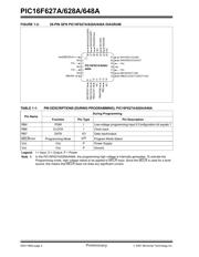
PIC16F627A/628A/648A
2.0 PROGRAM DETAILS
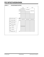
2.1 User Program Memory Map
The user memory space extends from 0x0000 to
0x1FFF. In Programming mode, the program memory
space extends from 0x0000 to 0x3FFF, with the first
half (0x0000-0x1FFF) being user program memory and
the second half (0x2000-0x3FFF) being configuration
memory. In the user program memory space, the PC
will increment from 0x0000 to the end of implemented
user program memory (see Figure 2-1) and wraps
around to 0x0000. Additionally, the high order bit is not
affected by the Increment Address command. Thus, in
configuration memory, the PC increments from 0x2000
to 0x3FFF and wraps around to 0x2000 (not to
0x0000). The only way to set the PC back to user
program memory is to reset the part and re-enter
Program/Verify mode as described in Section 2.4
“Program/Verify Mode”.
Configuration memory space is entered via the Load
Configuration command (see Section 2.4.3 “Load
Data for Configuration Memory”). Only addresses
0x2000-0x200F of configuration memory space are
physically implemented. However, only locations
0x2000 through 0x2007 are available. Other locations
are reserved. Locations beyond 0x200F will physically
access user memory.
2.2 User ID Locations
A user may store identification information (user ID) in
four user ID locations. The user ID locations are
mapped in [0x2000 : 0x2003]. These locations read out
normally even after the code protection is enabled.
2.3 EE Data Memory
The EE Data memory space extends from 0x00 to
0xFF and is separate from both program memory
space and RAM space.
Only the lower 128 bytes are implemented in the
PIC16F627A/628A devices, while the PIC16F648A
implements the full 256 bytes.
Programming the EE Data memory uses the same PC
as program memory, though only the lower bits are
decoded and used.
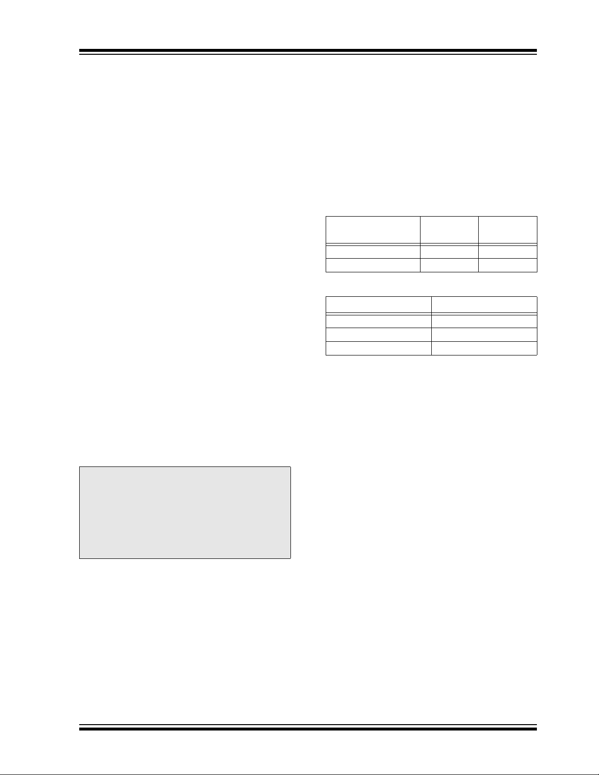
TABLE 2-1: EE DATA CAPACITY
TABLE 2-2: PROGRAM FLASH
Note 1: All other locations in PIC
®
MCU configu-
ration memory are reserved and should
not be programmed.
2: Only the low order 4 bits of the user ID
locations may be included in the device
checksum. See Section 3.10 “Check-
sum Computation” for checksum
calculation details.
Device
EE Data
Memory
PC Bits
Decoded
PIC16F627A/628A 128 7
PIC16F648A 256 8
Device Program Flash
PIC16F627A 1K
PIC16F628A 2K
PIC16F648A 4K
器件 Datasheet 文档搜索
AiEMA 数据库涵盖高达 72,405,303 个元件的数据手册,每天更新 5,000 多个 PDF 文件
