Datasheet 搜索 > 微控制器 > Microchip(微芯) > PIC16F716-I/P 数据手册 > PIC16F716-I/P 用户编程技术手册 4/18 页
 器件3D模型
¥ 10.39
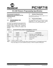
PIC16F716-I/P 用户编程技术手册 - Microchip(微芯)
制造商:
Microchip(微芯)
分类:
微控制器
封装:
PDIP-18
描述:
MICROCHIP PIC16F716-I/P 微控制器, 8位, 闪存, AEC-Q100, PIC16F, 20 MHz, 3.5 KB, 128 Byte, 18 引脚, DIP
Pictures:
3D模型
符号图
焊盘图
引脚图
产品图
页面导航:
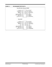
引脚图在P1P2Hot
电气规格在P16
导航目录
PIC16F716-I/P数据手册
Page:
of 18 Go
若手册格式错乱,请下载阅览PDF原文件
DS40245B-page 4 Preliminary 2003 Microchip Technology Inc.
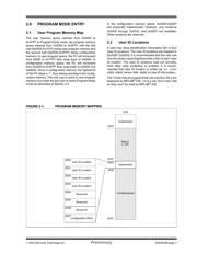
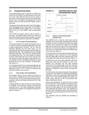
2.3 Program/Verify Mode
The Program/Verify mode is entered by holding pins
ICSPCLK and ICSPDAT low while raising V
DD pin from
V
IL to VDD. Then raise VPP from VIL to VIHH. Once in
this mode, the user program memory and configuration
memory can be accessed and programmed in serial
fashion. Clock and data are Schmitt Trigger inputs in
this mode.
The sequence that enters the device into the Program-
ming/Verify mode places all other logic into the RESET
state (the MCLR
pin was initially at VIL). This means
that all I/O are in the RESET state (hi-impedance
inputs).
The PIC16F716 program memory may be written in
two ways. The fastest method writes four words at a
time to the program memory array. However, one-word
writes are also supported for backward compatibility.
2.3.1 FOUR-WORD PROGRAMMING
The normal sequence for writing the program array is
to load four words to sequential addresses, then issue
a begin programming command. The PC must be
advanced following the first three loads, but not
advanced following the last program load until after the
programming cycle. The programming cycle is started
and timed externally. Then, the PC is advanced after
the programming cycle. The cycle repeats to program
the array. After writing the array, the PC may be reset
and the array may be read back to verify the write. It is
not possible to verify immediately following the write
because the PC can only increment, not decrement.
See Figure 2-11.
It is important that the PC is not advanced after the 4th
word is loaded as the programming cycle writes the row
selected by the PC <11:2>. If the PC is advanced, the
data will be written to the next row.
2.3.2 ONE-WORD PROGRAMMING
The program memory may be written one word at a
time to allow compatibility with some other PICmicro
®
FLASH devices. The one-word sequence loads a word,
programs, verifies, and finally increments the PC. See
Figure 2-10.
A device RESET will clear the PC and set the address
to ‘0x0000’. The Increment Address command will
increment the PC. The Load Configuration command
will set the PC to 0x2000. The available commands are
shown in Table 2-1.
FIGURE 2-2: ENTERING HIGH VOLTAGE
PROGRAM/VERIFY MODE
2.3.3 SERIAL PROGRAM/VERIFY
OPERATION
The ICSPCLK pin is used for clock input and the
ICSPDAT pin is used for data input/output during serial
operation. To input a command, the clock pin is cycled
six times. Each command bit is latched on the falling
edge of the clock with the LSb of the command being
input first. The data must adhere to the setup (T
SET1)
and hold (T
HLD1) times with respect to the falling edge
of the clock (see Table 5-1).
Commands that do not have data associated with them
are required to wait a minimum of T
DLY2 measured
from the falling edge of the last command clock to the
rising edge of the next command clock (see Table 5-1).
Commands that do have data associated with them
(Read and Load) are also required to wait T
DLY2
between the command and the data segment
measured from the falling edge of the last command
clock to the rising edge of the first data clock. The data
segment, consisting of 16 clock cycles, can begin after
this delay.
The first and last clock pulses during the data segment
correspond to the START and STOP bits respectively.
Input data is a don't care during the START and STOP
cycles. The 14 clock pulses between the START and
STOP cycles, clock the 14 bits of input/output data.
Data is transferred LSb first.
During read commands, in which the data is output
from the PIC16F716, the ICSPDAT pin transitions from
the hi-impedance state to the low impedance output
state at the rising edge of the second data clock (first
clock edge after the START cycle). The ICSPDAT pin
returns to the hi-impedance state at the rising edge of
the 16th data clock (first edge of the STOP cycle). See
Figure 2-5.
The commands that are available are described in
Table 2-1.
VPP
THLD0
ICSPDAT
ICSPCLK
VDD
TPPDP
器件 Datasheet 文档搜索
AiEMA 数据库涵盖高达 72,405,303 个元件的数据手册,每天更新 5,000 多个 PDF 文件
