Datasheet 搜索 > 8位微控制器 > Microchip(微芯) > PIC16F819-I/P 数据手册 > PIC16F819-I/P 用户编程技术手册 1/22 页
 器件3D模型
¥ 29.51
PIC16F819-I/P 用户编程技术手册 - Microchip(微芯)
制造商:
Microchip(微芯)
分类:
8位微控制器
封装:
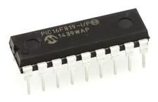
DIP-18
描述:
PIC16F818/819 8 位微控制器Microchip 的 PIC16F 系列微控制器 8 位 MCU,将 Microchip 的 PIC® 体系架构融入到引脚和封装选件中,从节省空间的 14 引脚设备到功能丰富的 64 引脚设备。 带有基线、中级或增强型中级体系架构的设备提供多种不同的外围设备组合,可谓设计人员提供灵活性,并为应用提供选择。 PIC16F818/819 系列微控制器基于 Microchip 中档内核,带 8 层深硬件堆栈和 35 个指令。 这些 MCU 提供高达 5 MIPS、14 K 字节程序内存和 368 字节 RAM。 板载是一个可配置振荡器,工厂校准到 ±1% 精确度。### 微控制器功能最大 20 MHz CPU 速度 35 个指令 8 级硬件堆栈 8 MHz 内部振荡器 – 可选频率 8 MHz 至 31 kHz 16 个输入/输出引脚 通电重置 (POR) 掉电重置 (BOR) 通电计时器 (PWRT) 振荡器启动计时器 (OST) 监控计时器 (WDT) 在线串行编程 (ICSP) 在线调试 (ICD) ### 外设5 通道 10 位模拟到数字转换器 (ADC) 捕获、比较、PWM (CCP) 模块 两个 8 位计时器 一个 16 位计时器 同步串行端口 (SSP),带有 SPI 和 I2C展开
Pictures:
3D模型
符号图
焊盘图
引脚图
产品图
页面导航:
引脚图在P3Hot
电气规格在P15


导航目录
PIC16F819-I/P数据手册
Page:
of 22 Go
若手册格式错乱,请下载阅览PDF原文件
2004 Microchip Technology Inc. DS39603C-page 1
M
PIC16F818/819
This document includes programming
specifications for the following devices:
• PIC16F818
• PIC16F819
1.0 PROGRAMMING THE
PIC16F818/819
The PIC16F818/819 is programmed using a serial
method. The Serial mode will allow the PIC16F818/819
to be programmed while in the user’s system, which
allows for increased design flexibility. This programming
specification applies to PIC16F818/819 devices in all
packages.
1.1 Programming Algorithm
Requirements
The programming algorithm used depends on the
operating voltage (V
DD) of the PIC16F818/819 device.
Both algorithms can be used with the two available
programming entry methods. The first method, called
Low-Voltage ICSP
TM
(LVP for short), applies VDD to
MCLR
and uses the I/O pin RB3 to enter Programming
mode. When RB3 is driven to V
DD from ground, the
PIC16F818/819 device enters Programming mode.
The second method follows the normal Microchip
Programming mode entry of holding pins RB6 and RB7
low, while raising the MCLR
pin from VIL to VIHH
(13V ± 0.5V).
1.2 Programming Mode
The Programming mode for the PIC16F818/819 allows
programming of user program memory, data memory,
special locations used for ID, and the configuration
word.
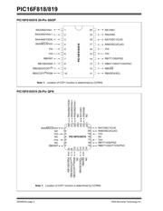
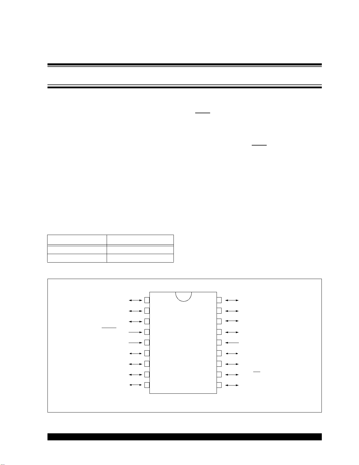
PIC16F818/819 18-Pin DIP, SOIC
Algorithm # VDD Range
12.0V≤ V
DD <5.5V
24.5V≤ V
DD ≤ 5.5V
RA1/AN1
RA0/AN0
RA7/OSC1/CLKI
RA6/OSC2/CLKO
V
DD
RB7/T1OSI/PGD
RB6/T1OSO/T1CKI/PGC
RB5/SS
RB4/SCK/SCL
RA2/AN2/VREF-
RA3/AN3/V
REF
+
RA4/AN4/T0CKI
RA5/MCLR
/VPP
V
SS
RB0/INT
RB1/SDI/SDA
RB2/SDO/CCP1
(1)
RB3/CCP1
(1)
/PGM
1
2
3
4
5
6
7
8
9
18
17
16
15
14
13
12
11
10
PIC16F818/819
Note 1: Location of CCP1 function is determined by CCPMX.
Flash Memory Programming Specification
器件 Datasheet 文档搜索
AiEMA 数据库涵盖高达 72,405,303 个元件的数据手册,每天更新 5,000 多个 PDF 文件
