Datasheet 搜索 > 8位微控制器 > Microchip(微芯) > PIC16F819-I/P 数据手册 > PIC16F819-I/P 用户编程技术手册 6/22 页
 器件3D模型
¥ 29.391
PIC16F819-I/P 用户编程技术手册 - Microchip(微芯)
制造商:
Microchip(微芯)
分类:
8位微控制器
封装:
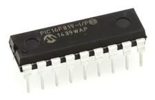
DIP-18
描述:
PIC16F818/819 8 位微控制器Microchip 的 PIC16F 系列微控制器 8 位 MCU,将 Microchip 的 PIC® 体系架构融入到引脚和封装选件中,从节省空间的 14 引脚设备到功能丰富的 64 引脚设备。 带有基线、中级或增强型中级体系架构的设备提供多种不同的外围设备组合,可谓设计人员提供灵活性,并为应用提供选择。 PIC16F818/819 系列微控制器基于 Microchip 中档内核,带 8 层深硬件堆栈和 35 个指令。 这些 MCU 提供高达 5 MIPS、14 K 字节程序内存和 368 字节 RAM。 板载是一个可配置振荡器,工厂校准到 ±1% 精确度。### 微控制器功能最大 20 MHz CPU 速度 35 个指令 8 级硬件堆栈 8 MHz 内部振荡器 – 可选频率 8 MHz 至 31 kHz 16 个输入/输出引脚 通电重置 (POR) 掉电重置 (BOR) 通电计时器 (PWRT) 振荡器启动计时器 (OST) 监控计时器 (WDT) 在线串行编程 (ICSP) 在线调试 (ICD) ### 外设5 通道 10 位模拟到数字转换器 (ADC) 捕获、比较、PWM (CCP) 模块 两个 8 位计时器 一个 16 位计时器 同步串行端口 (SSP),带有 SPI 和 I2C展开
Pictures:
3D模型
符号图
焊盘图
引脚图
产品图
页面导航:
引脚图在P3Hot
电气规格在P15


导航目录
PIC16F819-I/P数据手册
Page:
of 22 Go
若手册格式错乱,请下载阅览PDF原文件

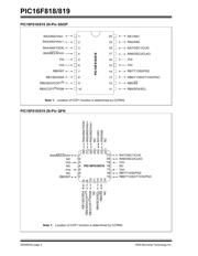
PIC16F818/819
DS39603C-page 6 2004 Microchip Technology Inc.
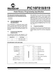
2.4.2 SERIAL PROGRAM OPERATION
The RB6 pin is used as a clock input pin, while the RB7
pin is used to enter command bits, and input or output
data during serial operation. To input a command, the
clock pin (RB6) is cycled six times. Each command bit
is latched on the falling edge of the clock, with the Least
Significant bit (LSb) of the command being input first.
The data on RB7 is required to have a minimum setup
(tset1) and hold (thold1) time (see AC/DC
specifications), with respect to the falling edge of the
clock. Commands with associated data (read and load)
are specified to have a minimum delay (tdly1) of 1 µs
between the command and the data. After this delay,
the clock pin is cycled 16 times, with the first cycle
being a Start bit (0) and the last cycle being a Stop bit
(0). Data is transferred LSb first.
During a read operation, the LSb will be transmitted
onto RB7 on the rising edge of the second cycle, while,
during a load operation, the LSb will be latched on the
falling edge of the second cycle. A minimum 1 µs delay
(tdly2) is specified between consecutive commands.
All commands and data words are transmitted LSb first.
The data is transmitted on the rising edge, and latched
on the falling edge of the clock. To allow decoding of
commands and reversal of data pin configuration, a
time separation of at least 1 µs (tdly1) is required
between a command and a data word, or another
command.
The available commands are described in the following
paragraphs and listed in Table 2-1.
2.4.2.1 Load Configuration
Upon receipt of the Load Configuration command, the
PC will be set to 0x2000 and the data sent with the
command is discarded. The four ID locations and the
configuration word can then be programmed using the
normal programming sequence, as described in
Section 2.4 “Program Mode”. A description of the
memory mapping schemes of the program memory for
normal operation and Configuration mode operation is
shown in Figure 2-1. Once the configuration memory is
entered, the only way to get back to the user program
memory is to exit the Program/Verify Test mode by
taking MCLR
low (V
IL
).
2.4.2.2 Load Data for Program Memory
After receiving this command, the chip will load one
word (with 14 bits as a “data word”) to be programmed
into user program memory when 16 cycles are applied.
A timing diagram for this command is shown in
Figure 6-1.
2.4.2.3 Load Data for Data Memory
After receiving this command, the chip will load a 14-bit
“data word” when 16 cycles are applied. However, the
data memory is only 8 bits wide and, thus, only the first
8 bits of data after the Start bit will be programmed into
the data memory (8 data bits and 6 zeros). It is still
necessary to cycle the clock the full 16 cycles in order
to allow the internal circuitry to reset properly. The data
memory contains up to 256 bytes. If the device is code
protected, the data is read as all zeros. A timing
diagram for this command is shown in Figure 6-2.
2.4.2.4 Read Data from Program Memory
After receiving this command, the chip will transmit
data bits out of the program memory (user or
configuration) currently accessed, starting with the
second rising edge of the clock input. The RB7 pin will
go into Output mode on the second rising clock edge,
reverting back to Input mode (high-impedance) after
the 16th rising edge. A timing diagram of this command
is shown in Figure 6-3.
2.4.2.5 Read Data from Data Memory
After receiving this command, the chip will transmit data
bits out of the data memory, starting with the second ris-
ing edge of the clock input. The RB7 pin will go into Out-
put mode on the second rising edge, reverting back to
Input mode (high-impedance) after the 16th rising edge.
As previously stated, the data memory is 8-bits wide
and, therefore, only the first 8 bits that are output are
actual data. A timing diagram for this command is
shown in Figure 6-4.
2.4.2.6 Increment Address
The PC is incremented when this command is
received. A timing diagram of this command is shown
in Figure 6-5.
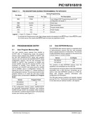
Note: Upon entry into Programming mode, a
“Load Data for Program Memory” or “Load
Data for Data Memory” command of 0x01
must be given before a Begin Erase or
Begin Programming command is initiated.
This will ensure that the programming
pointer is pointing to the correct location in
data or program memory.
器件 Datasheet 文档搜索
AiEMA 数据库涵盖高达 72,405,303 个元件的数据手册,每天更新 5,000 多个 PDF 文件
