Datasheet 搜索 > 32位控制器 > Microchip(微芯) > PIC32MX320F128HT-80I/MR 数据手册 > PIC32MX320F128HT-80I/MR 用户编程技术手册 5/76 页
 器件3D模型
¥ 14.58
PIC32MX320F128HT-80I/MR 用户编程技术手册 - Microchip(微芯)
制造商:
Microchip(微芯)
分类:
32位控制器
封装:
QFN-64
描述:
32位微控制器 - MCU 64Pin, 128 KB Flash 16 KB RAM, 80 MHz
Pictures:
3D模型
符号图
焊盘图
引脚图
产品图
页面导航:
引脚图在P5P6Hot
原理图在P9P72P74
电气规格在P7P8P63
导航目录
PIC32MX320F128HT-80I/MR数据手册
Page:
of 76 Go
若手册格式错乱,请下载阅览PDF原文件
2007-2016 Microchip Technology Inc. DS60001145S-page 5
PIC32
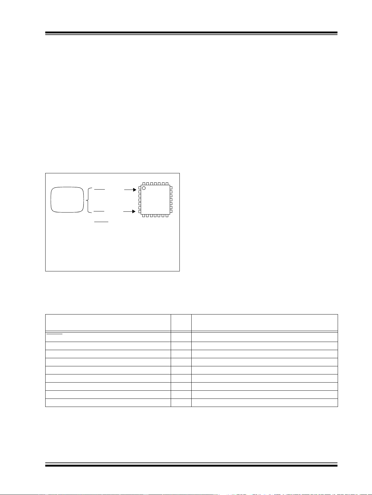
4.0 CONNECTING TO THE DEVICE
The PIC32 family provides two possible physical
interfaces for connecting and programming the
memory contents, see Figure 4-1. For all programming
interfaces, the target device must be powered and all
required signals must be connected. In addition, the
interface must be enabled, either through its
Configuration bit, as in the case of the JTAG 4-wire
interface, or though a special initialization sequence, as
is the case for the 2-wire ICSP interface.
The JTAG interface is enabled by default in blank
devices shipped from the factory.
Enabling ICSP is described in Section 7.0 “Entering
2-Wire Enhanced ICSP Mode”.
FIGURE 4-1: PROGRAMMING
INTERFACES
4.1 4-wire Interface
One possible interface is the 4-wire JTAG (IEEE
1149.1) port. Table 4-1 lists the required pin
connections. This interface uses the following four
communication lines to transfer data to and from the
PIC32 device being programmed:
• Test Clock Input (TCK)
• Test Mode Select Input (TMS)
• Test Data Input (TDI)
• Test Data Output (TDO)
Refer to the specific device data sheet for the
connection of the signals to the device pins.
4.1.1 TEST CLOCK INPUT (TCK)
TCK is the clock that controls the updating of the TAP
controller and the shifting of data through the Instruc-
tion or selected Data registers. TCK is independent of
the processor clock with respect to both frequency and
phase.
4.1.2 TEST MODE SELECT INPUT (TMS)
TMS is the control signal for the TAP controller. This
signal is sampled on the rising edge of TCK.
4.1.3 TEST DATA INPUT (TDI)
TDI is the test data input to the Instruction or selected
Data register. This signal is sampled on the rising edge
of TCK for some TAP controller states.
4.1.4 TEST DATA OUTPUT (TDO)
TDO is the test data output from the Instruction or Data
registers. This signal changes on the falling edge of
TCK. TDO is only driven when data is shifted out,
otherwise the TDO is tri-stated.
TABLE 4-1: 4-WIRE INTERFACE PINS
Programmer
2-wire
ICSP™
OR
4-wire
JTAG
+
MCLR, V
DD
1
V
8
(1)
,V
DDR
1
V
8
(1)
,
PIC32
V
DD
, V
SS
, V
SS
1
V
8
(1)
Note 1: This pin is not available on all devices.
Refer to the “Pin Diagrams” or “Pin
Tables” section in the specific device data
sheet to determine availability.
Device Pin Name
Pin
Type
Pin Description
MCLR
I Programming Enable
ENVREG
(2)
I Enable for On-Chip Voltage Regulator
V
DD
, V
DD
1
V
8
(2)
, V
DDR
1
V
8
(2)
, V
BAT
(2)
, and AV
DD
(1)
P Power Supply
V
SS
, V
SS
1
V
8
(2)
, and AV
SS
(1)
P Ground
V
CAP
(2)
P CPU logic filter capacitor connection
TDI I Test Data In
TDO O Test Data Out
TCK I Test Clock
TMS I Test Mode State
Legend: I = Input O = Output P = Power
Note 1: All power supply and ground pins must be connected, including analog supplies (AV
DD
) and ground (AV
SS
).
2: This pin is not available on all devices. Refer to the “Pin Diagrams” or “Pin Tables” section in the specific
device data sheet to determine availability.
器件 Datasheet 文档搜索
AiEMA 数据库涵盖高达 72,405,303 个元件的数据手册,每天更新 5,000 多个 PDF 文件
