Datasheet 搜索 > 微控制器 > Microchip(微芯) > ATTINY167-A15MD 数据手册 > ATTINY167-A15MD 其他数据使用手册 2/10 页

¥ 12.317
ATTINY167-A15MD 其他数据使用手册 - Microchip(微芯)
制造商:
Microchip(微芯)
分类:
微控制器
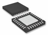
封装:
QFN
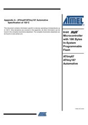
Pictures:
3D模型
符号图
焊盘图
引脚图
产品图
ATTINY167-A15MD数据手册
Page:
of 10 Go
若手册格式错乱,请下载阅览PDF原文件
2
7792B–AVR–05/09
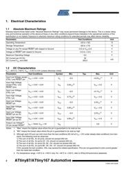
ATtiny87/ATtiny167 Automotive
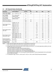
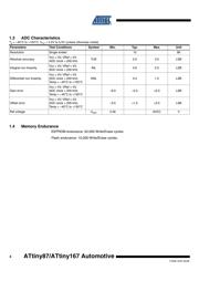
1. Electrical Characteristics
1.1 Absolute Maximum Ratings
Stresses beyond those listed under “Absolute Maximum Ratings” may cause permanent damage to the device. This is a stress rating
only and functional operation of the device at these or any other conditions beyond those indicated in the operational sections of this
specification is not implied. Exposure to absolute maximum rating conditions for extended periods may affect device reliability.
Parameters Test Conditions Unit
Operating Temperature –55 to +150 °C
Storage Temperature –65 to +175 °C
Voltage on any Pin except RESET
with respect to Ground –0.5 to V
CC
+0.5 V
Voltage on RESET
with respect to Ground –0.5 to +13.0 V
Maximum Operating Voltage 6.0 V
DC Current per I/O Pin
DC Current V
CC
and GND
30
200.0
mA
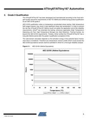
1.2 DC Characteristics
T
A
= –40°C to +150°C, V
CC
= 4.5V to 5.5V (unless otherwise noted)
Parameters Test Conditions Symbol Min. Typ. Max. Unit
Input Low Voltage, except
XTAL1 and RESET
pin
V
CC
= 4.5V – 5.5V V
IL
–0.5 +0.2V
CC
(1)
V
Input High Voltage,
except XTAL1 and
RESET
pins
V
CC
= 4.5V – 5.5V V
IH
0.6V
CC
(2)
V
CC
+ 0.5 V
Input Low Voltage,
XTAL1 pin
V
CC
= 4.5V – 5.5V V
IL1
–0.5 +0.1V
CC
(1)
V
Input High Voltage,
XTAL1 pin
V
CC
= 4.5V – 5.5V V
IH1
0.7V
CC
(2)
V
CC
+ 0.5 V
Input Low Voltage,
RESET
pin
V
CC
= 4.5V – 5.5V V
IL2
–0.5 0.2V
CC
(1)
V
Input High Voltage,
RESET pin
V
CC
= 4.5V – 5.5V V
IH2
0.9V
CC
(2)
V
CC
+ 0.5 V
Input Low Voltage,
RESET pin as I/O
V
CC
= 4.5V – 5.5V V
IL3
–0.5 0.2V
CC
(1)
V
Input High Voltage,
RESET
pin as I/O
V
CC
= 4.5V – 5.5V V
IH3
0.8V
CC
(2)
V
CC
+ 0.5 V
Output Low Voltage
(3)
,
I/O pin except RESET
I
OL
= 10mA, V
CC
= 5V V
OL
0.8 V
Notes: 1. “Max” means the highest value where the pin is guaranteed to be read as low
2. “Min” means the lowest value where the pin is guaranteed to be read as high
3. Although each I/O port can sink more than the test conditions (20 mA at V
CC
= 5V) under steady state conditions (non-tran-
sient), the following must be observed:
1] The sum of all IOL, for all ports, should not exceed 400 mA.
2] The sum of all IOL, for ports C0 - C5, should not exceed 200 mA.
3] The sum of all IOL, for ports C6, D0 - D4, should not exceed 300 mA.
4] The sum of all IOL, for ports B0 - B7, D5 - D7, should not exceed 300 mA.
If IOL exceeds the test condition, VOL may exceed the related specification. Pins are not guaranteed to sink current greater
than the listed test condition.
4. For temperature range +125°C to +150°C only. For –40°C to +125°C, refer to ATtiny167automotive datasheet.
器件 Datasheet 文档搜索
AiEMA 数据库涵盖高达 72,405,303 个元件的数据手册,每天更新 5,000 多个 PDF 文件
