Datasheet 搜索 > 微控制器 > NXP(恩智浦) > LPC2364FBD100 数据手册 > LPC2364FBD100 产品手册 1/48 页
 器件3D模型
¥ 49.411
LPC2364FBD100 产品手册 - NXP(恩智浦)
制造商:
NXP(恩智浦)
分类:
微控制器
封装:
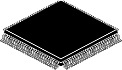
LQFP-100
描述:
ARM7 系列微控制器,NXP一系列 NXP 微控制器,基于 16/32 位 ARM7TDMI-S CPU ,带实时仿真和嵌入式追踪支持,将微控制器与 32 kB、64 kB、128 kB、256 kB 和 512 KB 嵌入式高速闪存相结合。 128 位宽存储器接口和独特的加速器体系结构实现在最大时钟频率时使用 32 位代码。高集成和低功耗 一系列串行通信接口和片上 SRAM 选项 备选 16 位 Thumb 模式将代码缩小 30%,而性能削弱最少。 32 位计时器,PWM 通道和多达 47 条 GPIO 线路 适用于工业控制和医疗系统 ### ARM7/9 微控制器,NXP
Pictures:
3D模型
符号图
焊盘图
引脚图
产品图
页面导航:
导航目录
LPC2364FBD100数据手册
Page:
of 48 Go
若手册格式错乱,请下载阅览PDF原文件

1. General description
The LPC2364/66/68 microcontrollers are based on a 16-bit/32-bit ARM7TDMI-S CPU with
real-time emulation that combines the microcontroller with up to 512 kB of embedded
high-speed flash memory. A 128-bit wide memory interface and a unique accelerator
architecture enable 32-bit code execution at the maximum clock rate. For critical
performance in interrupt service routines and DSP algorithms, this increases performance
up to 30 % over Thumb mode. For critical code size applications, the alternative 16-bit
Thumb mode reduces code by more than 30 % with minimal performance penalty.
The LPC2364/66/68 are ideal for multi-purpose serial communication applications. They
incorporate a 10/100 Ethernet Media Access Controller (MAC), USB full speed device
with 4 kB Endpoint RAM, four UARTs, two CAN channels, an SPI interface, two
Synchronous Serial Ports (SSP), three I
2
C interfaces, and an I
2
S interface. This blend of
serial communications interfaces combined with an on-chip 4 MHz internal oscillator,
SRAM of up to 32 kB, 16 kB SRAM for Ethernet, 8 kB SRAM for USB and general
purpose use, together with 2 kB battery powered SRAM make these devices very well
suited for communication gateways and protocol converters. Various 32-bit timers, an
improved 10-bit ADC, 10-bit DAC, one PWM unit, a CAN control unit, and up to 70 fast
GPIO lines with up to 12 edge or level sensitive external interrupt pins make these
microcontrollers particularly suitable for industrial control and medical systems.
2. Features
ARM7TDMI-S processor, running at up to 72 MHz.
Up to 512 kB on-chip Flash Program Memory with In-System Programming (ISP) and
In-Application Programming (IAP) capabilities. Flash program memory is on the ARM
local bus for high performance CPU access.
8/32 kB of SRAM on the ARM local bus for high performance CPU access.
16 kB SRAM for Ethernet interface. Can also be used as general purpose SRAM.
8 kB SRAM for general purpose DMA use also accessible by the USB.
Dual AHB system that provides for simultaneous Ethernet DMA, USB DMA, and
program execution from on-chip Flash with no contention between those functions. A
bus bridge allows the Ethernet DMA to access the other AHB subsystem.
Advanced Vectored Interrupt Controller, supporting up to 32 vectored interrupts.
General Purpose AHB DMA controller (GPDMA) that can be used with the SSP serial
interfaces, the I
2
S port, and the SD/MMC card port, as well as for memory-to-memory
transfers.
Serial Interfaces:
LPC2364/66/68
Single-chip 16-bit/32-bit microcontrollers; up to 512 kB flash
with ISP/IAP, Ethernet, USB 2.0, CAN, and 10-bit ADC/DAC
Rev. 01 — 22 September 2006 Preliminary data sheet
器件 Datasheet 文档搜索
AiEMA 数据库涵盖高达 72,405,303 个元件的数据手册,每天更新 5,000 多个 PDF 文件
