Datasheet 搜索 > 微控制器 > NXP(恩智浦) > LPC2364FBD100 数据手册 > LPC2364FBD100 产品手册 2/48 页
 器件3D模型
¥ 49.44
LPC2364FBD100 产品手册 - NXP(恩智浦)
制造商:
NXP(恩智浦)
分类:
微控制器
封装:
LQFP-100
描述:
ARM7 系列微控制器,NXP一系列 NXP 微控制器,基于 16/32 位 ARM7TDMI-S CPU ,带实时仿真和嵌入式追踪支持,将微控制器与 32 kB、64 kB、128 kB、256 kB 和 512 KB 嵌入式高速闪存相结合。 128 位宽存储器接口和独特的加速器体系结构实现在最大时钟频率时使用 32 位代码。高集成和低功耗 一系列串行通信接口和片上 SRAM 选项 备选 16 位 Thumb 模式将代码缩小 30%,而性能削弱最少。 32 位计时器,PWM 通道和多达 47 条 GPIO 线路 适用于工业控制和医疗系统 ### ARM7/9 微控制器,NXP
Pictures:
3D模型
符号图
焊盘图
引脚图
产品图
页面导航:
导航目录
LPC2364FBD100数据手册
Page:
of 48 Go
若手册格式错乱,请下载阅览PDF原文件

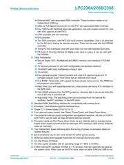
LPC2364_66_68_1 © Koninklijke Philips Electronics N.V. 2006. All rights reserved.
Preliminary data sheet Rev. 01 — 22 September 2006 2 of 48
Philips Semiconductors
LPC2364/2366/2368
Fast communication chip
Ethernet MAC with associated DMA controller. These functions reside on an
independent AHB bus.
USB 2.0 Full-Speed Device with on-chip PHY and associated DMA controller.
Four UARTs with fractional baud rate generation, one with modem control I/O, one
with IrDA support, all with FIFO.
CAN controller with two channels.
SPI controller.
Two SSP controllers, with FIFO and multi-protocol capabilities. One is an alternate
for the SPI port, sharing its interrupt and pins. These can be used with the GPDMA
controller.
Three I
2
C-bus interfaces (one with open-drain and two with standard port pins).
I
2
S (Inter-IC Sound) interface for digital audio input or output. It can be used with
the GPDMA.
Other Peripherals:
Secure Digital (SD) / MultiMediaCard (MMC) memory card interface (LPC2368
only).
70 General purpose I/O pins with configurable pull-up/down resistors.
10-bit ADC with input multiplexing among 6 pins.
10-bit DAC.
Four general purpose Timers/Counters with total of 8 capture inputs and 10
compare outputs. Each Timer block has an external count input.
One PWM / Timer block with support for three-phase motor control. The PWM has
two external count inputs.
Real Time Clock with separate power pin, clock source can be the RTC oscillator or
the APB clock.
2 kB SRAM powered from the RTC power pin, allowing data to be stored when the
rest of the chip is powered off.
Watchdog Timer. The watchdog timer can be clocked from the internal RC
oscillator, the RTC oscillator, or the APB clock.
Standard ARM Test/Debug interface for compatibility with existing tools.
Emulation Trace Module supports real-time trace.
Single 3.3 V power supply (3.0 V to 3.6 V).
Four reduced power modes, Idle, Sleep, Power Down, and Deep Power down.
Four external interrupt inputs configurable as edge/level sensitive. All pins on PORT0
and PORT2 can be used as edge sensitive interrupt sources.
Processor wake-up from Power-down mode via any interrupt able to operate during
Power-down mode (includes external interrupts, RTC interrupt, USB activity, Ethernet
wake-up interrupt).
Two independent power domains allow fine tuning of power consumption based on
needed features.
Each peripheral has its own clock divider for further power saving.
Brownout detect with separate thresholds for interrupt and forced reset.
On-chip Power On Reset.
On-chip crystal oscillator with an operating range of 1 MHz to 24 MHz.
4 MHz internal RC oscillator trimmed to 1 % accuracy that can optionally be used as
the system clock. When used as the CPU clock, does not allow CAN and USB to run.
器件 Datasheet 文档搜索
AiEMA 数据库涵盖高达 72,405,303 个元件的数据手册,每天更新 5,000 多个 PDF 文件
