Datasheet 搜索 > 微处理器 > NXP(恩智浦) > MPC8349EVVAJFB 数据手册 > MPC8349EVVAJFB 产品描述及参数 3/12 页
 器件3D模型
¥ 1520.719
MPC8349EVVAJFB 产品描述及参数 - NXP(恩智浦)
制造商:
NXP(恩智浦)
分类:
微处理器
封装:
BGA-672
描述:
PowerPC系列 533MHz
Pictures:
3D模型
符号图
焊盘图
引脚图
产品图
MPC8349EVVAJFB数据手册
Page:
of 12 Go
若手册格式错乱,请下载阅览PDF原文件
Instruction and Data Cache Locking on the e300 Processor Core, Rev. 1
Freescale Semiconductor 3
Set Up Memory
3Set Up Memory
For the cache locking example in this document, two areas of memory are defined through the BAT
registers:
• A 1 Mbyte area in the upper region of memory that contains the code for cache locking. It must be
cache-inhibited for instruction cache locking.
• A 256 Mbyte block of memory that contains the data to lock (not all of the 256 Mbyte of memory
is locked in the cache; this area is set up as an example).
Both memory areas use identity translation (the logical memory address equals the physical memory
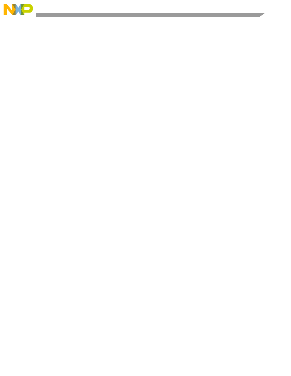
address). Table 2 summarizes the BAT settings for this example.
General block address translation (BAT) programming is beyond the scope of this document. For a full
discussion of BAT register programming, see the Programming Environments Manual for 32-Bit
Implementations of the PowerPC™ Architecture (MPCFPE32B), which is available at the web site listed
on the back cover of this document.
The block address translation upper (BATU) and block address translation lower (BATL) settings in
Table 2 are for both instruction block address translation (IBAT) and data block address translation
(DBAT) registers. After the BAT registers are set up, the MMU must be enabled. The following assembly
code enables both instruction and data memory address translation:
# Enable the instruction and data caches. This corresponds
# to setting the ICE and DCE bits in HID0 (bits 16 and 17)
mfspr r1, HID0
ori r1, r1, 0xc000
sync
mtspr HID0, r1
# Enable instruction and data memory address translation. This
# corresponds to setting IR and DR in the MSR (bits 26 & 27)
mfmsr r1
ori r1, r1, 0x0030
mtmsr r1
sync
Table 2. Example BAT Settings for Cache Locking
Area Base Address Memory Size WIMG Bits BATU Setting BATL Setting
First 0xFFF0_0000 1 Mbyte 0b0100
1
0xFFF0_001F 0xFFF0_0022
1
1
0xFFF0_0022 defines a cache-inhibited memory area for instruction cache locking and corresponds to a WIMG of 0b0100.
Cache-inhibited memory is not a requirement for data cache locking. A value of 0xFFF0_0002 with a corresponding WIMG of
0b0000 marks the memory area as cacheable.
Second 0x0000_0000 256 Mbyte 0b0000 0x0000_1FFF 0x0000_0002
器件 Datasheet 文档搜索
AiEMA 数据库涵盖高达 72,405,303 个元件的数据手册,每天更新 5,000 多个 PDF 文件
