Datasheet 搜索 > FET驱动器 > TI(德州仪器) > UCC27424DGNRG4 数据手册 > UCC27424DGNRG4 其他数据使用手册 3/34 页

¥ 5.925
UCC27424DGNRG4 其他数据使用手册 - TI(德州仪器)
制造商:
TI(德州仪器)
分类:
FET驱动器
封装:
PowerPad-MSOP-8
描述:
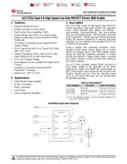
双4 -A高速低侧MOSFET驱动器与启用 Dual 4-A High Speed Low-Side MOSFET Drivers With Enable
Pictures:
3D模型
符号图
焊盘图
引脚图
产品图
页面导航:
引脚图在P3Hot
典型应用电路图在P14P15P16P17P18
原理图在P12
封装尺寸在P23P24P26P27
标记信息在P23P24P25
封装信息在P22P23P24P25P26P27
功能描述在P12
技术参数、封装参数在P4
应用领域在P1P25P34
电气规格在P5
导航目录
UCC27424DGNRG4数据手册
Page:
of 34 Go
若手册格式错乱,请下载阅览PDF原文件
ENBA
INA
GND
INB
ENBB
OUTA
VDD
OUTB
8
7
6
5
1
2
3
4
ENBA
INA
GND
INB
ENBB
OUTA
VDD
OUTB
8
7
6
5
1
2
3
4
ENBA
INA
GND
INB
ENBB
OUTA
VDD
OUTB
8
7
6
5
1
2
3
4
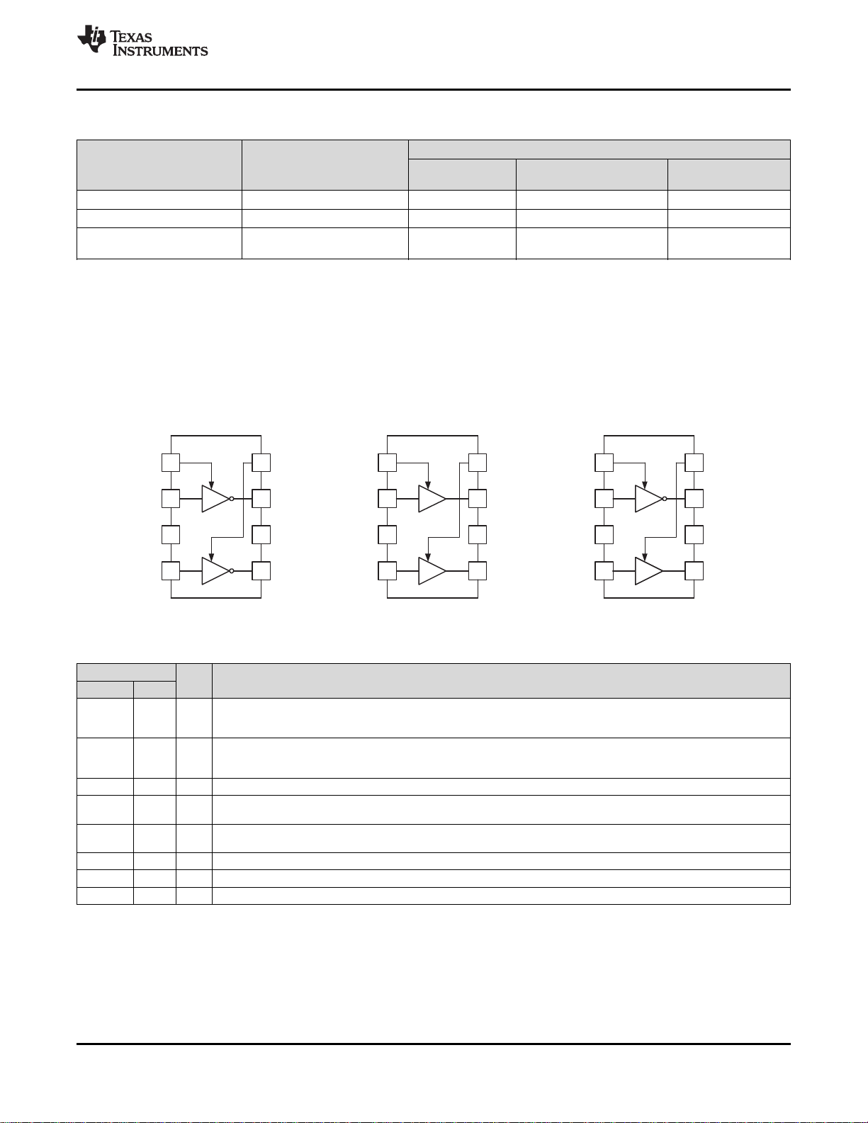
(DUAL INVERTING) (DUAL NON-INVERTING) (ONE INVERTING AND
ONE NON-INVERTING)
UCC27423
UCC27424
UCC27425
UCC27423
,
UCC27424
,
UCC27425
www.ti.com
SLUS545E –NOVEMBER 2002–REVISED DECEMBER 2015
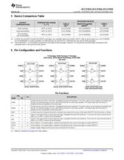
5 Device Comparison Table
PACKAGED DEVICES
OUTPUT TEMPERATURE RANGE
SOIC-8 MSOP-8 PowerPAD PDIP-8
CONFIGURATION T
A
= T
J
(D)
(1)
(DGN)
(2)
(P)
Dual inverting –40°C to 125°C UCC27423D UCC27423DGN UCC27423P
Dual nonInverting –40°C to 125°C UCC27424D UCC27424DGN UCC27424P
One inverting,
–40°C to 125°C UCC27425D UCC27425DGN UCC27425P
one noninverting
(1) D (SOIC-8) and DGN (PowerPAD-MSOP) packages are available taped and reeled. Add R suffix to device type (e.g. UCC27423DR,
UCC27424DGNR) to order quantities of 2,500 devices per reel for D or 1,000 devices per reel for DGN package.
(2) The PowerPAD™ is not directly connected to any leads of the package. However, it is electrically and thermally connected to the
substrate which is the ground of the device.
6 Pin Configuration and Functions
D Package, DGN Package, P Package
8-Pin SOIC, 8-PIn MSOP-PowerPAD, 8-Pin PDIP
Top View
Pin Functions
PIN
I/O DESCRIPTION
NAME NO.
Enable input for the driver A with logic compatible threshold and hysteresis. The driver output can be enabled and disabled with
ENBA 1 I this pin. It is internally pulled up to V
DD
with 100 kΩ resistor for active high operation. The output state when the device is
disabled will be low regardless of the input state.
Enable input for the driver B with logic compatible threshold and hysteresis. The driver output can be enabled and disabled with
ENBB 8 I this pin. It is internally pulled up to V
DD
with 100 kΩ resistor for active high operation. The output state when the device is
disabled will be low regardless of the input state.
(1)
GND 3 — Common ground: this ground should be connected very closely to the source of the power MOSFET which the driver is driving.
Input A: input signal of the A driver which has logic compatible threshold and hysteresis. If not used, this input should be tied to
INA 2 I
either V
DD
or GND. It should not be left floating.
(1)
Input B. Input signal of the A driver which has logic compatible threshold and hysteresis. If not used, this input should be tied to
INB 4 I
either V
DD
or GND. It should not be left floating.
OUTA 7 O Driver output A. The output stage is capable of providing 4A drive current to the gate of a power MOSFET.
OUTB 5 O Driver output B. The output stage is capable of providing 4A drive current to the gate of a power MOSFET.
V
DD
6 I Supply. Supply voltage and the power input connection for this device.
(1) Refer to Detailed Description for more details.
Copyright © 2002–2015, Texas Instruments Incorporated Submit Documentation Feedback 3
Product Folder Links: UCC27423 UCC27424 UCC27425
器件 Datasheet 文档搜索
AiEMA 数据库涵盖高达 72,405,303 个元件的数据手册,每天更新 5,000 多个 PDF 文件
