Datasheet 搜索 > FET驱动器 > TI(德州仪器) > UCC27424DGNRG4 数据手册 > UCC27424DGNRG4 其他数据使用手册 4/34 页

¥ 5.919
UCC27424DGNRG4 其他数据使用手册 - TI(德州仪器)
制造商:
TI(德州仪器)
分类:
FET驱动器
封装:
PowerPad-MSOP-8
描述:
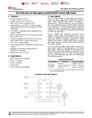
双4 -A高速低侧MOSFET驱动器与启用 Dual 4-A High Speed Low-Side MOSFET Drivers With Enable
Pictures:
3D模型
符号图
焊盘图
引脚图
产品图
页面导航:
引脚图在P3Hot
典型应用电路图在P14P15P16P17P18
原理图在P12
封装尺寸在P23P24P26P27
标记信息在P23P24P25
封装信息在P22P23P24P25P26P27
功能描述在P12
技术参数、封装参数在P4
应用领域在P1P25P34
电气规格在P5
导航目录
UCC27424DGNRG4数据手册
Page:
of 34 Go
若手册格式错乱,请下载阅览PDF原文件
UCC27423
,
UCC27424
,
UCC27425
SLUS545E –NOVEMBER 2002–REVISED DECEMBER 2015
www.ti.com
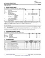
7 Specifications
7.1 Absolute Maximum Ratings
over operating free-air temperature range (unless otherwise noted)
(1)(2)
MIN MAX UNIT
V
DD
Supply voltage –0.3 16 V
I
OUT_DC
Output current (OUTA, OUTB) DC 0.2 A
I
OUT_PULSED
Pulsed, (0.5 μs) 4.5 A
V
IN
Input voltage (INA, INB) –5 6 or V
DD
+ 0.3 (whichever is larger) V
Enable voltage (ENBA, ENBB) –0.3 6 or V
DD
+ 0.3 (whichever is larger) V
DGN package 3 W
Power dissipation at
D package 650
T
A
= 25°C
mW
P package 350
T
J
Junction operating temperature –55 150 °C
Lead temperature (soldering, 10 s) 300 °C
T
stg
Storage temperature –65 150 °C
(1) Stresses beyond those listed under Absolute Maximum Ratings may cause permanent damage to the device. These are stress ratings
only, which do not imply functional operation of the device at these or any other conditions beyond those indicated under Recommended
Operating Conditions. Exposure to absolute-maximum-rated conditions for extended periods may affect device reliability.
(2) When V
DD
≤ 6 V, EN rating max value is 6 V; when V
DD
> 6 V, EN rating max value is V
DD
+ 0.3 V.
7.2 ESD Ratings
VALUE UNIT
Human body model (HBM), per ANSI/ESDA/JEDEC JS-001
(1)
±2500
V
(ESD)
Electrostatic discharge V
Charged device model (CDM), per JEDEC specification JESD22-C101
(2)
±1500
(1) JEDEC document JEP155 states that 500-V HBM allows safe manufacturing with a standard ESD control process.
(2) JEDEC document JEP157 states that 250-V CDM allows safe manufacturing with a standard ESD control process.
7.3 Recommended Operating Conditions
over operating free-air temperature range (unless otherwise noted)
MIN NOM MAX UNIT
V
DD
Supply voltage 4 15 V
INA and INB Input voltage –2 15 V
ENA and ENB Enable voltage 0 15 V
T
J
Operating junction temperature –40 125 °C
7.4 Thermal Information
UCC2742x
THERMAL METRIC
(1)
D (SOIC) DGN (MSOP) P (PDIP) UNIT
8 PINS 8 PINS 8 PINS
R
θJA
Junction-to-ambient thermal resistance 107.3 56.6 55.5 °C/W
R
θJC(top)
Junction-to-case (top) thermal resistance 52.2 52.8 45.3 °C/W
R
θJB
Junction-to-board thermal resistance 47.3 32.6 32.6 °C/W
ψ
JT
Junction-to-top characterization parameter 10.2 1.8 23.0 °C/W
ψ
JB
Junction-to-board characterization parameter 46.8 32.3 32.5 °C/W
R
θJC(bot)
Junction-to-case (bottom) thermal resistance – 5.9 – °C/W
(1) For more information about traditional and new thermal metrics, see the Semiconductor and IC Package Thermal Metrics application
report, SPRA953.
4 Submit Documentation Feedback Copyright © 2002–2015, Texas Instruments Incorporated
Product Folder Links: UCC27423 UCC27424 UCC27425
器件 Datasheet 文档搜索
AiEMA 数据库涵盖高达 72,405,303 个元件的数据手册,每天更新 5,000 多个 PDF 文件
