Datasheet 搜索 > TI(德州仪器) > CDCLVD110 数据手册 > CDCLVD110 用户编程技术手册 3/14 页

¥ 0
CDCLVD110 用户编程技术手册 - TI(德州仪器)
制造商:
TI(德州仪器)
描述:
具有最低时钟失真斜率最高 900MHz 的 1 至 10 LVDS 时钟缓冲器
Pictures:
3D模型
符号图
焊盘图
引脚图
产品图
页面导航:
导航目录
CDCLVD110数据手册
Page:
of 14 Go
若手册格式错乱,请下载阅览PDF原文件
www.ti.com
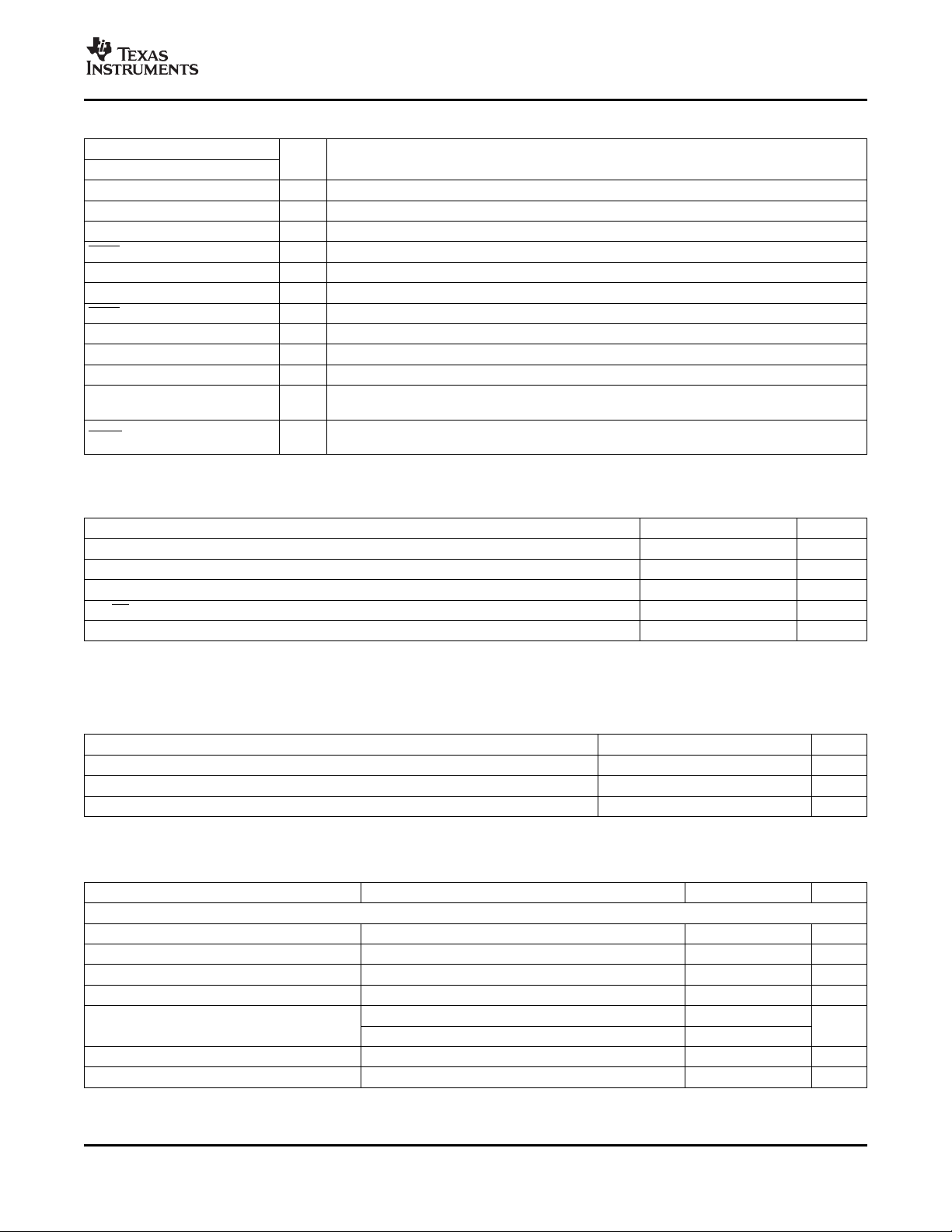
ABSOLUTE MAXIMUM RATINGS
(1)
RECOMMENDED OPERATING CONDITIONS
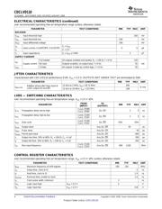
ELECTRICAL CHARACTERISTICS
CDCLVD110
SCAS684C – SEPTEMBER 2002 – REVISED JANUARY 2008
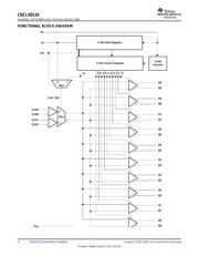
TERMINAL FUNCTIONS
TERMINAL
I/O DESCRIPTION
NAME NO.
CK 1 I Control register input clock, features a 120-k Ω pullup resistor
SI 2 I Control register serial input/CLK Select, features a 120-k Ω pulldown resistor
CLK0 3 I True differential input, LVDS
CLK0 4 I Complementary differential input, LVDS
V
BB
5 O Reference voltage output
CLK1 6 I True differential input, LVDS
CLK1 7 I Complementary differential input, LVDS
EN 8 I Control enable (for programmability), features a 120-k Ω pulldown resistor, input
V
SS
9, 25 Device ground
V
DD
16, 32 Supply voltage
11, 13, 15, 18, 20, 22,
Q [9:0] O Clock outputs, these outputs provide low-skew copies of CLKIN
24, 27, 29, 31
10, 12, 14, 17, 19,
Q[9:0] O Complementary clock outputs, these outputs provide low-skew copies of CLKIN
21,23, 26, 28, 30
VALUE UNIT
V
DD
Supply voltage – 0.3 to 2.8 V
V
I
Input voltage – 0.2 to (V
DD
+ 0.2) V
V
O
VI Output voltage – 0.2 to (V
DD
+ 0.2) V
Qn, Qn, I
OSD
Driver short circuit current Continuous
Electrostatic discharge (HBM 1.5 k Ω , 100 pF), ESD >2000 V
(1) Stresses beyond those listed under absolute maximum ratings may cause permanent damage to the device. These are stress ratings
only, and functional operation of the device at these or any other conditions beyond those indicated under recommended operating
conditions is not implied. Exposure to absolute-maximum-rated conditions for extended periods may affect device reliability.
MIN NOM MAX UNIT
V
DD
Supply voltage 2.375 2.5 2.625 V
V
IC
Receiver common-mode input voltage 0.5|V
ID
| V
DD
– 0.5|V
ID
| V
T
A
Operating free-air temperature – 40 85 ° C
over recommended operating free-air temperature range (unless otherwise noted)
PARAMETER TEST CONDITIONS MIN TYP MAX UNIT
DRIVER
|V
OD
| Differential output voltage R
L
= 100 Ω 250 450 600 mV
Δ V
OD
V
OD
magnitude change 50 mV
V
OS
Offset voltage – 40 ° C to 85 ° C 0.95 1.2 1.45 V
Δ V
OS
V
OS
magnitude change 350 mV
V
O
= 0 V – 20
I
OS
Output short circuit current mA
|V
OD
| = 0 V 20
V
BB
Reference output voltage V
DD
= 2.5 V, I
BB
= – 100 µ A 1.15 1.25 1.35 V
C
O
Output capacitance V
O
= V
DD
or GND 3 pF
Copyright © 2002 – 2008, Texas Instruments Incorporated Submit Documentation Feedback 3
Product Folder Link(s) :CDCLVD110
器件 Datasheet 文档搜索
AiEMA 数据库涵盖高达 72,405,303 个元件的数据手册,每天更新 5,000 多个 PDF 文件
