Datasheet 搜索 > TI(德州仪器) > CDCLVD110 数据手册 > CDCLVD110 用户编程技术手册 5/14 页

¥ 0
CDCLVD110 用户编程技术手册 - TI(德州仪器)
制造商:
TI(德州仪器)
描述:
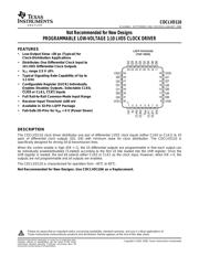
具有最低时钟失真斜率最高 900MHz 的 1 至 10 LVDS 时钟缓冲器
Pictures:
3D模型
符号图
焊盘图
引脚图
产品图
页面导航:
导航目录
CDCLVD110数据手册
Page:
of 14 Go
若手册格式错乱,请下载阅览PDF原文件
www.ti.com
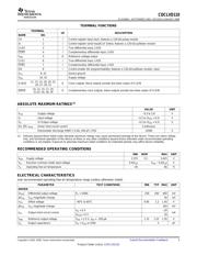
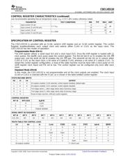
SPECIFICATION OF CONTROL REGISTER
CDCLVD110
SCAS684C – SEPTEMBER 2002 – REVISED JANUARY 2008
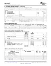
CONTROL REGISTER CHARACTERISTICS (continued)
over recommended operating free-air temperature range, V
DD
= 2.5 V ± 5% (unless otherwise noted)
PARAMETER TEST CONDITIONS MIN TYP MAX UNIT
Input current, CK pin – 5 5
I
IH
V
I
= V
DD
µ A
Input current, SI and EN pins 10 – 30
Input current, CK pin – 10 30
I
IL
V
I
= GND µ A
Input current, SI and EN pins – 5 5
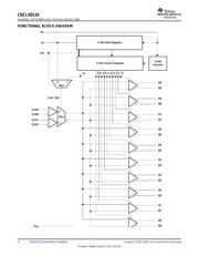
The CDCLVD110 is provided with an 11-bit, serial-in shift register and an 11-bit control register. The control
Register enables/disables each output clock and selects either CLK0 or CLK1 as the input clock. The
CDCLVD110 has two modes of operation:
Programmable Mode (EN=1)
The shift register utilizes a serial input (SI) and a clock input (CK). Once the shift register is loaded with 11
clock pulses, the twelfth clock pulse loads the control register. The first bit (bit 0) on SI enables the Q9, Q9
output pair, and the tenth bit (bit 9) enables the Q0, Q0 pair. The eleventh bit (bit 10) on SI selects either
CLK0 or CLK1 as the input clock; a bit value of 0 selects CLK0, whereas a bit value of 1 selects CLK1. To
restart the control register configuration, a reset of the state machine must be done with a clock pulse on CK
(shift register clock input) and EN set to low. The control register can be configured only once after each
reset.
Standard Mode (EN=0)
In this mode, the CDCLVD110 is not programmable and all the clock outputs are enabled. The clock input
(CLK0 or CLK1) is selected with the SI pin, as is shown in the table entitled control register.
STATE-MACHINE INPUTS
EN SI CK OUTPUT
L L X All outputs enabled, CLK0 selected, control register disabled, default state
L H X All outputs enabled, CLK1 selected, control register disabled
H L ↑ First stage stores L, other stage stores data of previous stage
H H First stage stores H, other stage stores data of previous stage
L X Reset of state machine, shift and control registers
CONTROL REGISTER
BIT 10 BITS [0-9] Q
N
[0-9]
L H CLK0
H H CLK1
X L Outputs disabled
SERIAL INPUT (SI) SEQUENCE
BIT 10 BIT 9 BIT 8 BIT 7 BIT 6 BIT 5 BIT 4 BIT 3 BIT 2 BIT 1 BIT 0
CLK_SEL Q0 Q1 Q2 Q3 Q4 Q5 Q6 Q7 Q8 Q9
TRUTH TABLE FOR CONTROL LOGIC
CK EN SI CLK0 CLK0 CLK1 CLK1 Q(0-9) Q(0-9)
L L L L H X X L H
L L L H L X X H L
L L L Open Open X X L H
L L H X X L H L H
L L H X X H L H L
L L H X X Open Open L H
All outputs enabled X = Don't care
Copyright © 2002 – 2008, Texas Instruments Incorporated Submit Documentation Feedback 5
Product Folder Link(s) :CDCLVD110
器件 Datasheet 文档搜索
AiEMA 数据库涵盖高达 72,405,303 个元件的数据手册,每天更新 5,000 多个 PDF 文件
