Datasheet 搜索 > TI(德州仪器) > CDCLVD110 数据手册 > CDCLVD110 用户编程技术手册 6/14 页

¥ 0
CDCLVD110 用户编程技术手册 - TI(德州仪器)
制造商:
TI(德州仪器)
描述:
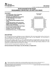
具有最低时钟失真斜率最高 900MHz 的 1 至 10 LVDS 时钟缓冲器
Pictures:
3D模型
符号图
焊盘图
引脚图
产品图
页面导航:
导航目录
CDCLVD110数据手册
Page:
of 14 Go
若手册格式错乱,请下载阅览PDF原文件

www.ti.com
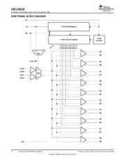
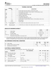
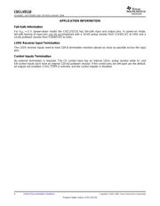
APPLICATION INFORMATION
Fall-Safe Information
LVDS Receiver Input Termination
Control Inputs Termination
CDCLVD110
SCAS684C – SEPTEMBER 2002 – REVISED JANUARY 2008
For V
DD
= 0 V (power-down mode) the CDCLVD110 has fail-safe input and output pins. In power-on mode,
fail-safe biasing at input pins can be accomplished with a 10-k Ω pullup resistor from CLK0/CLK1 to VDD and a
10-k Ω pulldown resistor from CLK0/ CLK1 to GND.
The LVDS receiver inputs need to have 100- Ω termination resistors placed as close as possible across the input
pins.
No external termination is required. The CK control input has an internal 120-k. pullup resistor while SI- and
EN-control inputs each have an internal 120-k Ω pulldown resistor. If the control pins are left open per the default,
all outputs are enabled, CLK0, CLK0 is selected, and the control register is disabled.
6 Submit Documentation Feedback Copyright © 2002 – 2008, Texas Instruments Incorporated
Product Folder Link(s) :CDCLVD110
器件 Datasheet 文档搜索
AiEMA 数据库涵盖高达 72,405,303 个元件的数据手册,每天更新 5,000 多个 PDF 文件
