Datasheet 搜索 > 16位微控制器 > NXP(恩智浦) > MC9S12A64CFUE 数据手册 > MC9S12A64CFUE 用户编程技术手册 2/60 页

 器件3D模型
¥ 150.801
MC9S12A64CFUE 用户编程技术手册 - NXP(恩智浦)
制造商:
NXP(恩智浦)
分类:
16位微控制器
封装:
QFP-80
描述:
NXP MC9S12A64CFUE 微控制器, 16位, S12A, 25 MHz, 64 KB, 4 KB, 80 引脚, QFP
Pictures:
3D模型
符号图
焊盘图
引脚图
产品图
页面导航:
应用领域在P1
导航目录
MC9S12A64CFUE数据手册
Page:
of 60 Go
若手册格式错乱,请下载阅览PDF原文件

Application Note
AN2153
2
Unlike the M68HC11 Family, the MC9S12DP256 does not have a
bootstrap ROM containing firmware to allow initial programming of the
FLASH directly through one of the on-chip serial communications
interface (SCI) ports. Initial on-chip FLASH programming requires either
special test and handling equipment to program the device before it is
placed in the target system or a background debug module (BDM)
programming tool available from Freescale or a third party vendor.
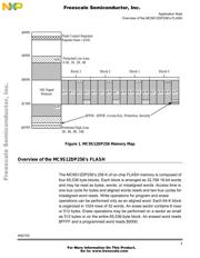
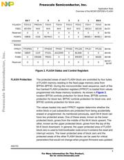
The MC9S12DP256’s four on-chip FLASH arrays contain two variable
size, erase protectable areas as shown in Figure 1. While the majority
of the bootloader could be contained in any of the protected areas, the
protected high area in the $C000–$FFFF memory range must at least
contain reset and interrupt vectors that point to a jump table. In most
cases, unless a complex or sophisticated communication protocol is
required that will not fit into 16 K, it is easiest to place the entire
bootloader into the protected high area of block zero.
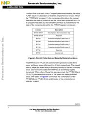
Erasing and programming the on-chip FLASH memory of the
MC9S12DP256 presents some unique challenges. Even though FLASH
block zero has two separate erase protected areas, code cannot be run
out of either protected area while the remainder of the block is erased or
programmed. While it is possible to run code from one FLASH block
while erasing or reprogramming another, adopting such a strategy would
complicate the overall implementation of the bootloader. Consequently,
during the erase and reprogram process, the code must reside in other
on-chip memory or in external memory. In addition, because the reset
and interrupt vectors reside in the erase protected area, they cannot be
changed. This necessitates a secondary reset/interrupt vector table be
placed outside the protected FLASH memory area.
The remainder of this application note explores the requirements of a
serial bootloader and the implementation of the programming algorithm
for the MC9S12DP256’s FLASH.
Freescale Semiconductor, I
Freescale Semiconductor, Inc.
For More Information On This Product,
Go to: www.freescale.com
nc
.
..
器件 Datasheet 文档搜索
AiEMA 数据库涵盖高达 72,405,303 个元件的数据手册,每天更新 5,000 多个 PDF 文件
