Datasheet 搜索 > 接口芯片 > TI(德州仪器) > TLK1102ERGER 数据手册 > TLK1102ERGER 数据手册 2/32 页
 器件3D模型
¥ 116.989
TLK1102ERGER 数据手册 - TI(德州仪器)
制造商:
TI(德州仪器)
分类:
接口芯片
封装:
VQFN-24
描述:
11.3 - Gbps的双通道电缆和PC主板均衡器 11.3-Gbps Dual-Channel Cable and PC Board Equalizer
Pictures:
3D模型
符号图
焊盘图
引脚图
产品图
页面导航:
封装尺寸在P26P27P28
封装信息在P26P27P28
应用领域在P32
导航目录
TLK1102ERGER数据手册
Page:
of 32 Go
若手册格式错乱,请下载阅览PDF原文件
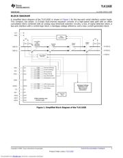
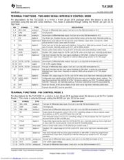
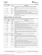
DESCRIPTION (CONTINUED)
TLK1102E
SLLS958 – MARCH 2009 ...................................................................................................................................................................................................
www.ti.com
These devices have limited built-in ESD protection. The leads should be shorted together or the device placed in conductive foam
during storage or handling to prevent electrostatic damage to the MOS gates.
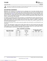
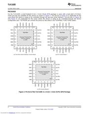
Alternatively, the TLK1102E can be configured using its configuration pins in two modes selectable using the
MODE pin. In Pin Control Mode 1 (see Figure 2 b), a common setting can be set for the two channels for the
output de-emphasis level and the interconnect length using the DE pin and LN0, LN1 pins respectively. In Pin
Control Mode 2 (see Figure 2 c), those parameters can be set individually for the two channels using DEA, DEB,
LNA, and LNB pins. In both modes only a common setting is available for the output voltage swing using the
SWG pin. For Pin Control Mode 2 the typical LOS assert and de-assert voltage levels are fixed at 90mV
p-p
and
150mV
p-p
respectively with 4.0dB hysteresis.
The outputs can be disabled using the DISA and DISB pins. The DISA/DISB pins and the LOSA/LOSB pins can
be connected together to implement an external output squelch function. The TLK1102E implements an internal
output squelch function that can be enabled using the two-wire serial interface. In addition, a special fast
auto-squelch function can be selected through the two-wire serial interface when needed to support SAS and
SATA out-of-band (OOB) signals.
The POLA and POLB pins can be used to reverse the polarity of the OUTA+/OUTA- and OUTB+/OUTB – pins
respectively.
The high input signal dynamic range ensures low jitter output signals even when overdriven with input signal
swings as high as 1600mV
p-p
differential. The low-frequency cut-off is low enough to support low-frequency
control signals such as SAS and SATA OOB signals. The loss-of-signal detection and output disable functions
are carefully designed to meet SAS/SATA OOB signal timing constraints.
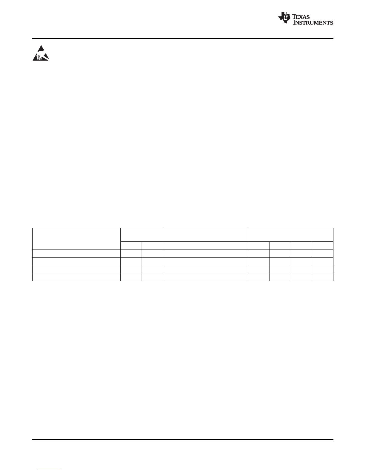
Table 1. Equalization Level Settings
TWO-WIRE SERIAL I/F MODE
PIN MODE 1 PIN MODE 2
CABLE LENGTH (meters)
(registers 3 and 6)
(1.8dB/m loss at 5 GHz)
LN1 LN0 LNA / LNB EQ3 EQ2 EQ1 EQ0
0 – 2 GND GND GND 1 1 1 1
2 – 6 GND VCC GND 0 1 1 1
6 – 11 VCC GND 1.8 M Ω to GND 0 1 0 1
11 – 15 VCC VCC VCC 0 0 0 0
2 Submit Documentation Feedback Copyright © 2009, Texas Instruments Incorporated
Product Folder Link(s): TLK1102E
Downloaded from Elcodis.com electronic components distributor
器件 Datasheet 文档搜索
AiEMA 数据库涵盖高达 72,405,303 个元件的数据手册,每天更新 5,000 多个 PDF 文件
