Datasheet 搜索 > 接口芯片 > TI(德州仪器) > TLK1102ERGER 数据手册 > TLK1102ERGER 数据手册 5/32 页
 器件3D模型
¥ 116.88
TLK1102ERGER 数据手册 - TI(德州仪器)
制造商:
TI(德州仪器)
分类:
接口芯片
封装:
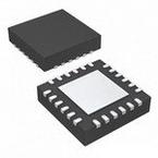
VQFN-24
描述:
11.3 - Gbps的双通道电缆和PC主板均衡器 11.3-Gbps Dual-Channel Cable and PC Board Equalizer
Pictures:
3D模型
符号图
焊盘图
引脚图
产品图
页面导航:
封装尺寸在P26P27P28
封装信息在P26P27P28
应用领域在P32
导航目录
TLK1102ERGER数据手册
Page:
of 32 Go
若手册格式错乱,请下载阅览PDF原文件
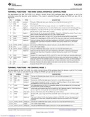
TERMINAL FUNCTIONS - TWO-WIRE SERIAL INTERFACE CONTROL MODE
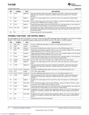
TERMINAL FUNCTIONS - PIN CONTROL MODE 1
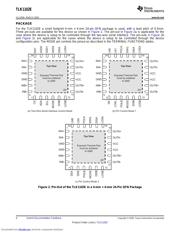
TLK1102E
www.ti.com
................................................................................................................................................................................................... SLLS958 – MARCH 2009
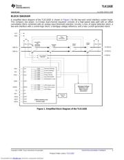
Pin descriptions for the TLK1102E in a 4-mm x 4-mm 24-pin QFN package when the device is set to be
controlled using the two-wire serial interface. This mode is selected through setting the MODE pin (pin 10) to
high level.
PIN SYMBOL TYPE DESCRIPTION
1, 2 INA+, INA- analog-in First pair of differential data inputs. Each pin is on-chip 50 Ω terminated to VCC.
3, 4 GND supply Circuit ground.
5, 6 INB+, INB- analog-in Second pair of differential data inputs. Each pin is on-chip 50 Ω terminated to VCC.
7 CS digital-in Chip Select pin. Disables the two-wire serial interface when set to low level. Internally pulled up.
8 SDA digital-in/out Bidirectional serial data pin for the two-wire serial interface. Open drain. Connect to a 10k Ω
pull-up resistor if used. Leave open if unused.
9 SCL digital-in Serial clock pin for the two-wire serial interface. Connect to a 10k Ω pull-up resistor if used. Leave
open if unused. Internally pulled up to VCC with a 500k Ω resistor.
10 MODE three-state Device control mode select. Pull up to VCC for the two-wire serial interface control mode.
11 DISB digital-in Disables CML output stage for OUTB+ and OUTB- when set to high level. Internally pulled down.
12 LOSB digital-out High level indicates that the input signal amplitude on INB+/INB- is below the programmed
threshold level. Open drain. Requires an external 10k Ω pull-up resistor to VCC for proper
operation.
13, 14 OUTB-, OUTB+ analog-out Second pair of differential data outputs. Each pin is on-chip 50 Ω terminated to VCC.
15, 16 VCC supply 3.3V ± 10% supply voltage.
17, 18 OUTA-, OUTA+ analog-out First pair of differential data outputs. Each pin is on-chip 50 Ω terminated to VCC.
19 LOSA digital-out High level indicates that the input signal amplitude on INA+/INA- is below the programmed
threshold level. Open drain. Requires an external 10k Ω pull-up resistor to VCC for proper
operation.
20 DISA digital-in Disables CML output stage for OUTA+ and OUTA- when set to high level. Internally pulled down.
21, 22, ADD2, ADD1, digital-in Configurable least significant bits (ADD[2:0]) of the two-wire serial interface device address. The
23 ADD0 fixed most significant bits (ADD[6:3]) of the 7-bit device address are 0101. The default address is
0101100. These pins are internally pulled up. Pull down externally to invert the associated bits.
24 RST digital-in Reset pin. Resets all the device digital circuits when set to high level. Internally pulled down.
EP EP Exposed die pad (EP) must be grounded.
Pin descriptions for the TLK1102E in a 4-mm x 4-mm 24-pin QFN package when the device is set for Pin Control
Mode 1. This mode is selected through setting the MODE pin (pin 10) to low level.
PIN SYMBOL TYPE DESCRIPTION
1, 2 INA+, INA- analog-in First pair of differential data inputs. Each pin is on-chip 50 Ω terminated to VCC.
3, 4 GND supply Circuit ground.
5, 6 INB+, INB- analog-in Second pair of differential data inputs. Each pin is on-chip 50 Ω terminated to VCC.
7 DE analog-in Output signal de-emphasis control. A 0 to 1.2-V controlling voltage on this pin adjusts output
de-emphasis on OUTA and OUTB pins from 0 to 7dB.
8 LOSL analog-in LOS threshold control. A 0 to 0.7-V controlling voltage on this pin adjusts the LOS assert and
de-assert levels on INA and INB pins.
9 POLB digital-in Output data signal polarity select for OUTB+/OUTB- pins. Internally pulled up. Set to high level
or leave open for normal polarity. Set to low level for inverted polarity.
10 MODE three-state Device control mode select. Tie to GND for pin control mode 1.
11 DISB digital-in Disables CML output stage for OUTB+ and OUTB- when set to high level. Internally pulled
down.
12 LOSB digital-out High level indicates that the input signal amplitude on INB+/INB- is below the programmed
threshold level. Open drain. Requires an external 10k Ω pull-up resistor to VCC for proper
operation.
13, 14 OUTB-, OUTB+ analog-out Second pair of differential data outputs. Each pin is on-chip 50 Ω terminated to VCC.
15, 16 VCC supply 3.3V ± 10% supply voltage.
17, 18 OUTA-, OUTA+ analog-out First pair of differential data outputs. Each pin is on-chip 50 Ω terminated to VCC.
Copyright © 2009, Texas Instruments Incorporated Submit Documentation Feedback 5
Product Folder Link(s): TLK1102E
Downloaded from Elcodis.com electronic components distributor
器件 Datasheet 文档搜索
AiEMA 数据库涵盖高达 72,405,303 个元件的数据手册,每天更新 5,000 多个 PDF 文件
