Datasheet 搜索 > 双极性晶体管 > ON Semiconductor(安森美) > D45H11G 数据手册 > D45H11G 其他数据使用手册 1/9 页

¥ 4.679
D45H11G 其他数据使用手册 - ON Semiconductor(安森美)
制造商:
ON Semiconductor(安森美)
分类:
双极性晶体管
封装:
TO-220-3
描述:
PNP 功率晶体管,ON Semiconductor### 标准带 NSV 前缀的制造商部件号具有汽车资格,符合 AEC-Q101 标准。### 双极性晶体管,On SemiconductorON Semiconductor 的各种双极晶体管,包括以下类别:小信号晶体管 通用晶体管 双 NPN 和 PNP 晶体管 功率晶体管 高电压晶体管 射频双极晶体管 低噪声,双匹配和复杂的双极晶体管
Pictures:
3D模型
符号图
焊盘图
引脚图
产品图
页面导航:
导航目录
D45H11G数据手册
Page:
of 9 Go
若手册格式错乱,请下载阅览PDF原文件
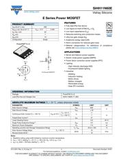
SiHH11N60E
www.vishay.com
Vishay Siliconix
S15-2031-Rev. A, 24-Aug-15
1
Document Number: 91651
For technical questions, contact: hvm@vishay.com
THIS DOCUMENT IS SUBJECT TO CHANGE WITHOUT NOTICE. THE PRODUCTS DESCRIBED HEREIN AND THIS DOCUMENT
ARE SUBJECT TO SPECIFIC DISCLAIMERS, SET FORTH AT www.vishay.com/doc?91000
E Series Power MOSFET
FEATURES
• Fully lead (Pb)-free device
• Low figure-of-merit (FOM) R
on
x Q
g
• Low input capacitance (C
iss
)
• Reduced switching and conduction losses
• Ultra low gate charge (Q
g
)
• Avalanche energy rated (UIS)
• Kelvin connection for reduced gate noise
• Material categorization: for definitions of compliance
please see www.vishay.com/doc?99912
APPLICATIONS
• Server and telecom power supplies
• Switch mode power supplies (SMPS)
• Power factor correction power supplies (PFC)
• Lighting
- High-intensity discharge (HID)
- Fluorescent ballast lighting
• Industrial
- Welding
- Induction heating
- Motor drives
- Battery chargers
- Renewable energy
- Solar (PV inverters)
Notes
a. Repetitive rating; pulse width limited by maximum junction temperature.
b. V
DD
= 140 V, starting T
J
= 25 °C, L = 28.2 mH, R
g
= 25 Ω, I
AS
= 3 A.
c. I
SD
≤ I
D
, dI/dt = 100 A/μs, starting T
J
= 25 °C.
PRODUCT SUMMARY
V
DS
(V) at T
J
max. 650
R
DS(on)
typ. (Ω) at 25 °C V
GS
= 10 V 0.295
Q
g
max. (nC) 62
Q
gs
(nC) 7
Q
gd
(nC) 13
Configuration Single
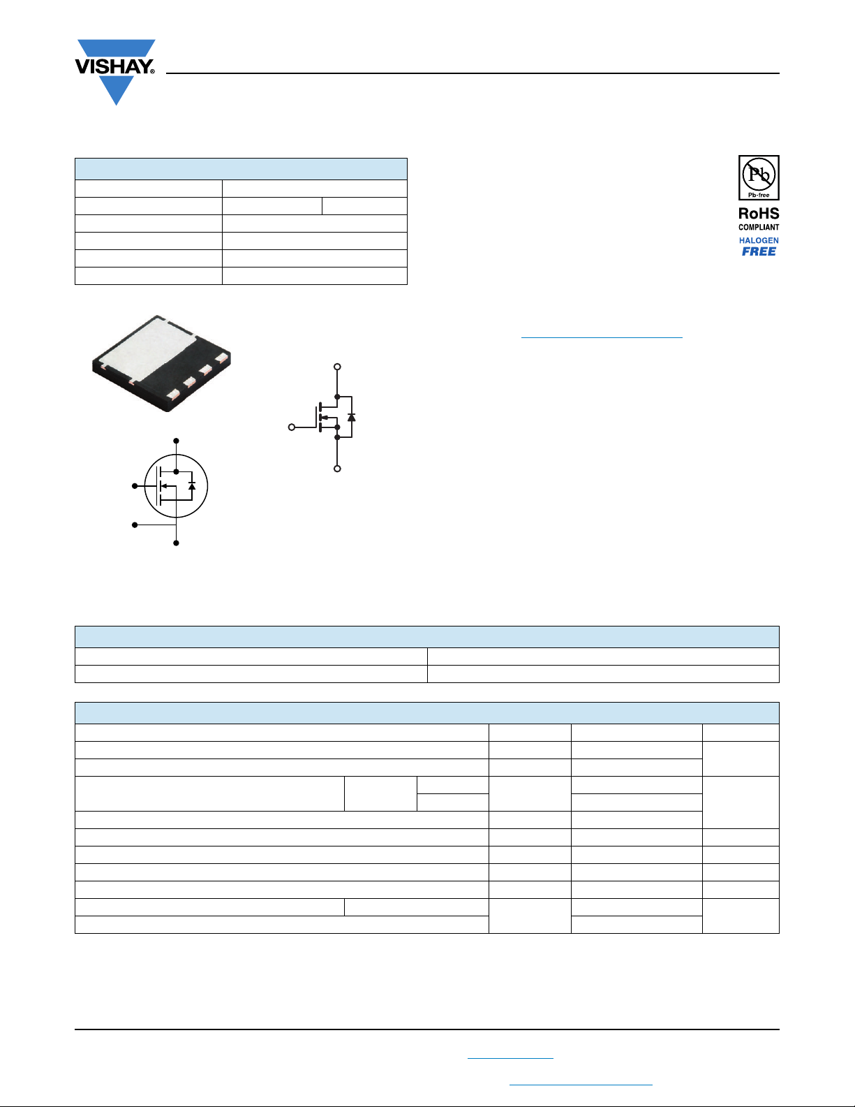
N-Channel MOSFET
G
D
S
PowerPAK
®
8 x 8
1
2
3
3
4
Pin 3
Pin 4
Pin 1
Pin 2
ORDERING INFORMATION
Package PowerPAK 8 x 8
Lead (Pb)-free and Halogen-free SiHH11N60E-T1-GE3
ABSOLUTE MAXIMUM RATINGS (T
C
= 25 °C, unless otherwise noted)
PARAMETER SYMBOL LIMIT UNIT
Drain-Source Voltage V
DS
600
V
Gate-Source Voltage V
GS
± 30
Continuous Drain Current (T
J
= 150 °C) V
GS
at 10 V
T
C
= 25 °C
I
D
11
AT
C
= 100 °C 7
Pulsed Drain Current
a
I
DM
27
Linear Derating Factor 0.9 W/°C
Single Pulse Avalanche Energy
b
E
AS
127 mJ
Maximum Power Dissipation P
D
114 W
Operating Junction and Storage Temperature Range T
J
, T
stg
-55 to +150 °C
Drain-Source Voltage Slope T
J
= 125 °C
dV/dt
70
V/ns
Reverse Diode dV/dt
c
18
器件 Datasheet 文档搜索
AiEMA 数据库涵盖高达 72,405,303 个元件的数据手册,每天更新 5,000 多个 PDF 文件
