Datasheet 搜索 > 双极性晶体管 > ON Semiconductor(安森美) > D45H11G 数据手册 > D45H11G 其他数据使用手册 2/9 页

¥ 4.663
D45H11G 其他数据使用手册 - ON Semiconductor(安森美)
制造商:
ON Semiconductor(安森美)
分类:
双极性晶体管
封装:
TO-220-3
描述:
PNP 功率晶体管,ON Semiconductor### 标准带 NSV 前缀的制造商部件号具有汽车资格,符合 AEC-Q101 标准。### 双极性晶体管,On SemiconductorON Semiconductor 的各种双极晶体管,包括以下类别:小信号晶体管 通用晶体管 双 NPN 和 PNP 晶体管 功率晶体管 高电压晶体管 射频双极晶体管 低噪声,双匹配和复杂的双极晶体管
Pictures:
3D模型
符号图
焊盘图
引脚图
产品图
页面导航:
导航目录
D45H11G数据手册
Page:
of 9 Go
若手册格式错乱,请下载阅览PDF原文件
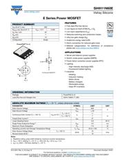
SiHH11N60E
www.vishay.com
Vishay Siliconix
S15-2031-Rev. A, 24-Aug-15
2
Document Number: 91651
For technical questions, contact: hvm@vishay.com
THIS DOCUMENT IS SUBJECT TO CHANGE WITHOUT NOTICE. THE PRODUCTS DESCRIBED HEREIN AND THIS DOCUMENT
ARE SUBJECT TO SPECIFIC DISCLAIMERS, SET FORTH AT www.vishay.com/doc?91000
Notes
a. C
oss(er)
is a fixed capacitance that gives the same energy as C
oss
while V
DS
is rising from 0 % to 80 % V
DS
.
b. C
oss(tr)
is a fixed capacitance that gives the same charging time as C
oss
while V
DS
is rising from 0 % to 80 % V
DS
.
THERMAL RESISTANCE RATINGS
PARAMETER SYMBOL TYP. MAX. UNIT
Maximum Junction-to-Ambient R
thJA
42 55
°C/W
Maximum Junction-to-Case (Drain)
R
thJC
0.76 1.10
SPECIFICATIONS (T
J
= 25 °C, unless otherwise noted)
PARAMETER SYMBOL TEST CONDITIONS MIN. TYP. MAX. UNIT
Static
Drain-Source Breakdown Voltage V
DS
V
GS
= 0 V, I
D
= 250 μA 600 - - V
V
DS
Temperature Coefficient ΔV
DS
/T
J
Reference to 25 °C, I
D
= 1 mA - 0.66 - V/°C
Gate-Source Threshold Voltage (N) V
GS(th)
V
DS
= V
GS
, I
D
= 250 μA 2.0 - 4.0 V
Gate-Source Leakage I
GSS
V
GS
= ± 20 V - - ± 100 nA
V
GS
= ± 30 V - - ± 1 μA
Zero Gate Voltage Drain Current I
DSS
V
DS
= 600 V, V
GS
= 0 V - - 1
μA
V
DS
= 480 V, V
GS
= 0 V, T
J
= 125 °C - - 50
Drain-Source On-State Resistance R
DS(on)
V
GS
= 10 V I
D
= 5.5 A - 0.295 0.339 Ω
Forward Transconductance g
fs
V
DS
= 30 V, I
D
= 5.5 A - 3.7 - S
Dynamic
Input Capacitance C
iss
V
GS
= 0 V,
V
DS
= 100 V,
f = 1 MHz
- 1076 -
pF
Output Capacitance C
oss
-56-
Reverse Transfer Capacitance C
rss
-6-
Effective Output Capacitance, Energy
Related
a
C
o(er)
V
DS
= 0 V to 480 V, V
GS
= 0 V
-52-
Effective Output Capacitance, Time
Related
b
C
o(tr)
- 174 -
Total Gate Charge Q
g
V
GS
= 10 V I
D
= 5.5 A, V
DS
= 480 V
-3162
nC Gate-Source Charge Q
gs
-7-
Gate-Drain Charge Q
gd
-13-
Turn-On Delay Time t
d(on)
V
DD
= 480 V, I
D
= 5.5 A,
V
GS
= 10 V, R
g
= 9.1 Ω
-1632
ns
Rise Time t
r
-2142
Turn-Off Delay Time t
d(off)
-3968
Fall Time t
f
-2142
Gate Input Resistance R
g
f = 1 MHz, open drain 0.2 0.7 1.5 Ω
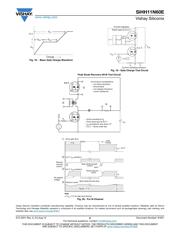
Drain-Source Body Diode Characteristics
Continuous Source-Drain Diode Current I
S
MOSFET symbol
showing the
integral reverse
p - n junction diode
--11
A
Pulsed Diode Forward Current I
SM
--27
Diode Forward Voltage V
SD
T
J
= 25 °C, I
S
= 5.5 A, V
GS
= 0 V - 0.9 1.2 V
Reverse Recovery Time t
rr
T
J
= 25 °C, I
F
= I
S
= 5.5 A,
dI/dt = 100 A/μs, V
R
= 25 V
- 280 560 ns
Reverse Recovery Charge Q
rr
-3.06.0μC
Reverse Recovery Current I
RRM
-20-A
S
D
G
器件 Datasheet 文档搜索
AiEMA 数据库涵盖高达 72,405,303 个元件的数据手册,每天更新 5,000 多个 PDF 文件
