Datasheet 搜索 > 微控制器 > NXP(恩智浦) > MC56F8006VLC 数据手册 > MC56F8006VLC 用户编程技术手册 5/106 页
 器件3D模型
¥ 26.727
MC56F8006VLC 用户编程技术手册 - NXP(恩智浦)
制造商:
NXP(恩智浦)
分类:
微控制器
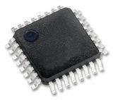
封装:
LQFP-32
描述:
NXP MC56F8006VLC 芯片, 数字信号控制器, 16位, 32MHZ, 16KB, 32LQFP
Pictures:
3D模型
符号图
焊盘图
引脚图
产品图
页面导航:
引脚图在P13Hot
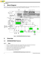
原理图在P4P9
封装尺寸在P18P19P20P21P22P23P24P25P26P27P28P73
型号编码规则在P72
技术参数、封装参数在P1P11P41P42P43P44P45P46P47P48P49P50
电气规格在P46P57
导航目录
MC56F8006VLC数据手册
Page:
of 106 Go
若手册格式错乱,请下载阅览PDF原文件

Overview
MC56F8006/MC56F8002 Digital Signal Controller, Rev. 4
Freescale Semiconductor 5
• Parallel instruction set with unique DSP addressing modes
• Hardware DO and REP loops
• Three internal address buses
• Four internal data buses
• Instruction set supports DSP and controller functions
• Controller-style addressing modes and instructions for compact code
• Efficient C compiler and local variable support
• Software subroutine and interrupt stack with depth limited only by memory
• JTAG/enhanced on-chip emulation (EOnCE) for unobtrusive, processor speed–independent, real-time debugging
3.1.2 Operation Range
• 1.8 V to 3.6 V operation (power supplies and I/O)
• From power-on-reset: approximately 1.9 V to 3.6 V
• Ambient temperature operating range:
— –40 °C to 125 °C
3.1.3 Memory
• Dual Harvard architecture permits as many as three simultaneous accesses to program and data memory
• Flash security and protection that prevent unauthorized users from gaining access to the internal flash
• On-chip memory
— 16 KB of program flash for 56F8006 and 12 KB of program flash for 56F8002
— 2 KB of unified data/program RAM
• EEPROM emulation capability using flash
3.1.4 Interrupt Controller
• Five interrupt priority levels
— Three user programmable priority levels for each interrupt source: Level 0, 1, 2
— Unmaskable level 3 interrupts include: illegal instruction, hardware stack overflow, misaligned data access, SWI3
instruction. Maskable level 3 interrupts include: EOnCE step counter, EOnCE breakpoint unit, EOnCE trace
buffer
— Lowest-priority software interrupt: level LP
• Allow nested interrupt that higher priority level interrupt request can interrupt lower priority interrupt subroutine
• The masking of interrupt priority level is managed by the 56800E core
• One programmable fast interrupt that can be assigned to any interrupt source
• Notification to system integration module (SIM) to restart clock out of wait and stop states
• Ability to relocate interrupt vector table
3.1.5 Peripheral Highlights
• One multi-function, six-output pulse width modulator (PWM) module
— Up to 96 MHz PWM operating clock
— 15 bits of resolution
— Center-aligned and edge-aligned PWM signal mode
— Phase shifting PWM pulse generation
器件 Datasheet 文档搜索
AiEMA 数据库涵盖高达 72,405,303 个元件的数据手册,每天更新 5,000 多个 PDF 文件
