Datasheet 搜索 > 微控制器 > NXP(恩智浦) > MC56F8006VLC 数据手册 > MC56F8006VLC 用户编程技术手册 6/106 页
 器件3D模型
¥ 26.727
MC56F8006VLC 用户编程技术手册 - NXP(恩智浦)
制造商:
NXP(恩智浦)
分类:
微控制器
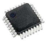
封装:
LQFP-32
描述:
NXP MC56F8006VLC 芯片, 数字信号控制器, 16位, 32MHZ, 16KB, 32LQFP
Pictures:
3D模型
符号图
焊盘图
引脚图
产品图
页面导航:
引脚图在P13Hot
原理图在P4P9
封装尺寸在P18P19P20P21P22P23P24P25P26P27P28P73
型号编码规则在P72
技术参数、封装参数在P1P11P41P42P43P44P45P46P47P48P49P50
电气规格在P46P57
导航目录
MC56F8006VLC数据手册
Page:
of 106 Go
若手册格式错乱,请下载阅览PDF原文件

MC56F8006/MC56F8002 Digital Signal Controller, Rev. 4
Overview
Freescale Semiconductor6
— Four programmable fault inputs with programmable digital filter
— Double-buffered PWM registers
— Separate deadtime insertions for rising and falling edges
— Separate top and bottom pulse-width correction by means of software
— Asymmetric PWM output within both Center Aligned and Edge Aligned operation
— Separate top and bottom polarity control
— Each complementary PWM signal pair allows selection of a PWM supply source from:
– PWM generator
– Internal timers
– Analog comparator outputs
• Two independent 12-bit analog-to-digital converters (ADCs)
— 2 x 14 channel external inputs plus seven internal inputs
— Support simultaneous and software triggering conversions
— ADC conversions can be synchronized by PWM and PDB modules
— Sampling rate up to 400 KSPS for 10- or 12-bit conversion result; 470 KSPS for 8-bit conversion result
— Two 16-word result registers
• Two programmable gain amplifier (PGAs)
— Each PGA is designed to amplify and convert differential signals to a single-ended value fed to one of the ADC
inputs
— 1X, 2X, 4X, 8X, 16X, or 32X gain
— Software and hardware triggers are available
— Integrated sample/hold circuit
— Includes additional calibration features:
– Offset calibration eliminates any errors in the internal reference used to generate the VDDA/2 output center
point
– Gain calibration can be used to verify the gain of the overall datapath
– Both features require software correction of the ADC result
• Three analog comparators (CMPs)
— Selectable input source includes external pins, internal DACs
— Programmable output polarity
— Output can drive timer input, PWM fault input, PWM source, external pin output, and trigger ADCs
— Output falling and rising edge detection able to generate interrupts
• One dual channel 16-bit multi-purpose timer module (TMR)
— Two independent 16-bit counter/timers with cascading capability
— Up to 96 MHz operating clock
— Each timer has capture and compare and quadrature decoder capability
— Up to 12 operating modes
— Four external inputs and two external outputs
• One serial communication interface (SCI) with LIN slave functionality
— Up to 96 MHz operating clock
— Full-duplex or single-wire operation
— Programmable 8- or 9- bit data format
— Two receiver wakeup methods:
– Idle line
– Address mark
器件 Datasheet 文档搜索
AiEMA 数据库涵盖高达 72,405,303 个元件的数据手册,每天更新 5,000 多个 PDF 文件
